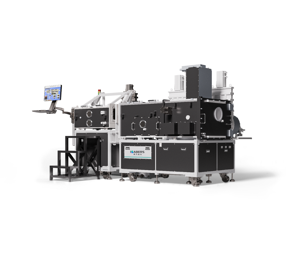
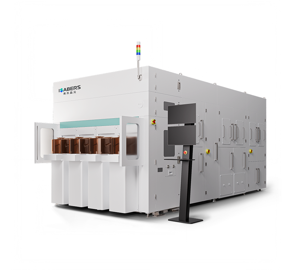


Features
-

- Broad Chip Size Compatibility
- Optimized chip pick and place technology supports chip thickness down to 35μm, size spanning 1*1mm to 32*32mm.
-

- Alignment Modes Compatibility
- Inter-chip coaxial alignment: Bonding accuracy ≤±500 nm. Infrared penetration alignment: Bonding accuracy ≤±200 nm.
-

- Optional Bottom-to-top Bonding
- In addition to top-to-bottom bonding, the system offers bottom-to-top bonding, that the wafer bonding face remains downward, eliminating the need for chip flipping, thus significantly reducing particle contamination risks.
-

- Real-time Overlay Measurement & Feedback Control
- Instant post-bonding overlay measurement, with automatic algorithmic compensation in subsequent bonding steps, ensures consistent bonding accuracy.
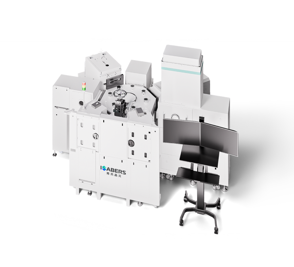
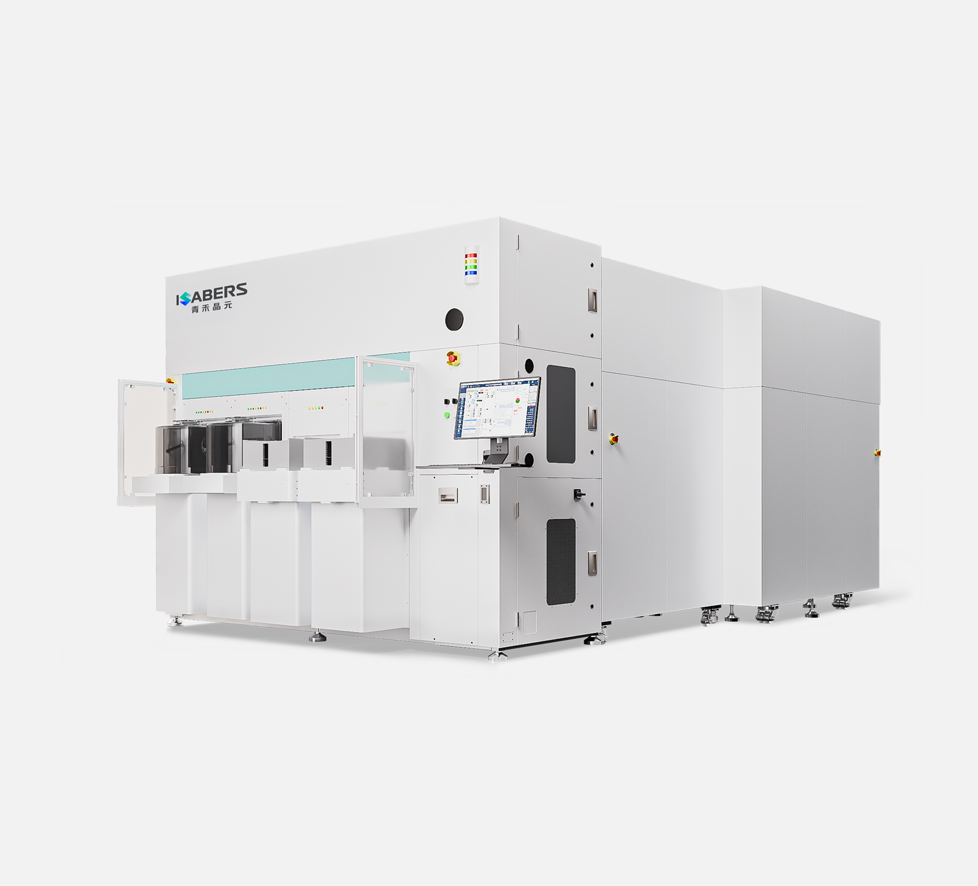
Specifications
-
ItemsSpecification
-
TF loadport2
-
FOUP loadport2
-
Bonding force rangeMax 30N
-
Post-bonding accuracy≤±500 nm@ Inter-chip coaxial alignment
≤±200 nm@ Infrared transmissive alignment -
Chip size5*8 mm—32*32 mm
1*1 mm—32*32 mm -
Wafer size8/12 inch
-
UPHSingle bonding head: >800@200 nm@3σ
Single bonding head: >400@50 nm@3σ -
ProcessCu/SiO₂ hybrid bonding, Cu/SiCN hybrid bonding
-
Multi-module integratedActivation, clean, UV debond, chip pick and place, alignment, bonding, and detection