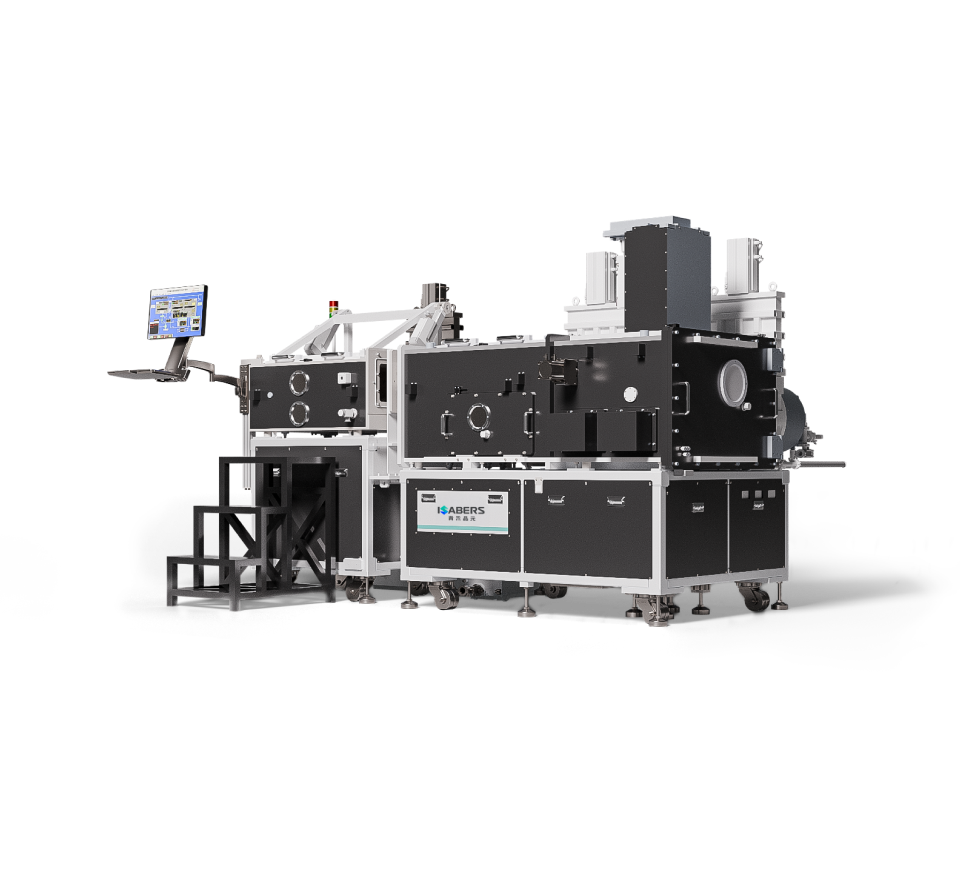
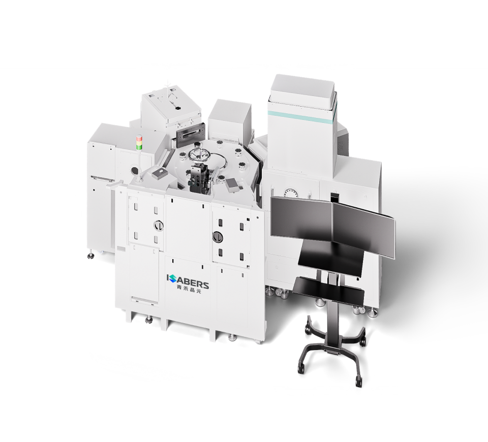
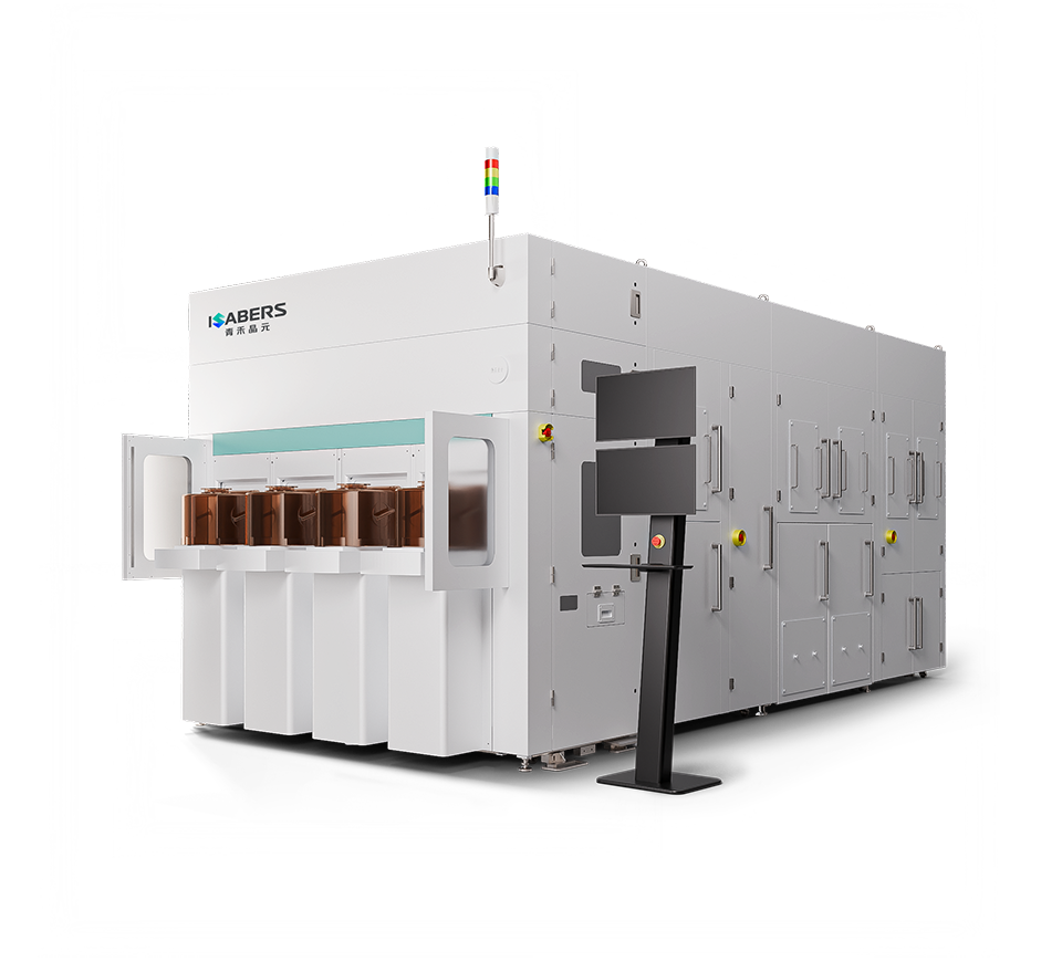
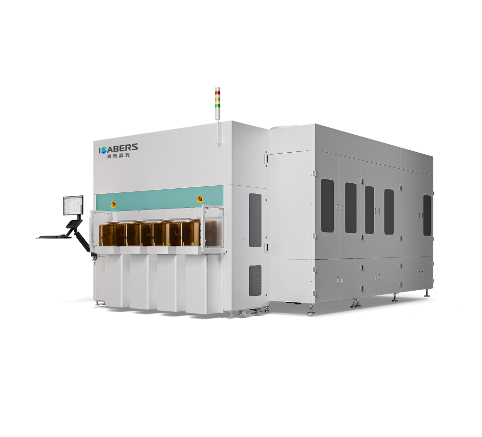

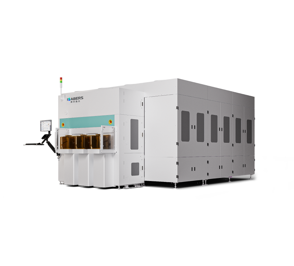


Features
-

- Real-time Automated Leveling & Alignment
- Automated leveling between chips and wafers with real-time parallelism monitoring at bonding positions, achievs bonding accuracy up to ±500 nm.
-

- Dual Activation Modes
- Independent hydrogen radical and plasma activation chambers. Hydrogen radicals enable low-temperature reduction (at 180°C) on metal surfaces (e.g., Cu).
-

- Rapid heating/cooling capability
- Heats from RT to 450°C in ≤2.2s, and gas-accelerated cools, minimizing thermal mismatch deformation, preventing bump shorting, and improving bonding efficiency.
-

- Full-process Inert Atmosphere
- Post-activation transfer and bonding occur entirely in an inert atmosphere to avoid air exposure and oxidation, ensuring higher bonding quality.
Specifications
-
ItemsSpecification
-
Bonding force range and stabilityOption 1: -30-500 N (0.25 N or 1%)
Option 2: 10-3000 N (±2 N) -
Chip size0.4*0.4-32*32/0.4*0.4-50*50/1*1-70*70 mm
-
C2S type lower wafer size10*10 mm-120*300 mm
-
C2W type lower wafer size8, 12 inch
-
Bonder temperatureRT~450℃
-
Bonder stability±0.5℃
-
Bonder heating rate (RT-450 ℃)2.2s @ 32*32 mm
-
Post-bonding accuracy≤±2 μm; ≤±1 μm; ≤±500 nm
-
Activation chamber atmosphereHydrogen radical activation, plasma activation.
-
Bond chamber atmosphereInert atmosphere