


- Process Capabilities
Process Capabilities
-

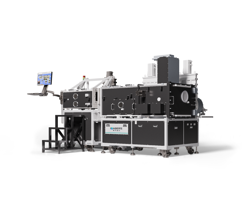
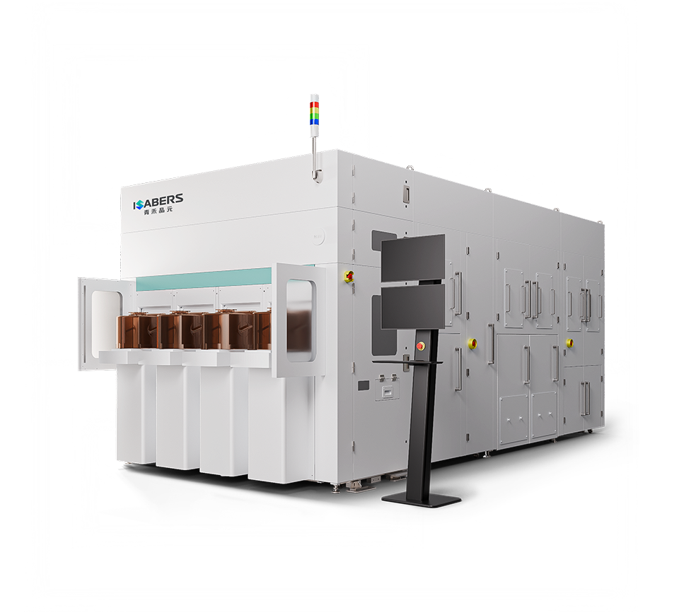
- Ion Implantation
- Ion Implanter
- Wafer size: 4, 6, 8, 12 inch and non-standard shaped materials
- Implant energy: 5-210 keV
- Implant dose: 5E11-1E17 ions/cm²
- Implant angle: Tilt: 0°-60°, Twist: 0°-359°
- Processed wafer types: SiC, Si, LN, LT, Diamond
- Main Function:
- Complete the doping modification of H, P, and He elements through ion implanting.
-

- Bonding
- Room-Temperature Bonding Machine
- Wafer Size: 4, 6, 8 inch
- Wafer Thickness: <1000 µm
- Alignment Accuracy: X, Y ≤ 70 μm, θ ≤ 0.2 deg
- Bonding Energy: 1.0-2.0 J/m²
- Processed Wafer Types: 4H-SiC, Poly-SiC, Si, SiO₂, LT, LN, Quartz, Glass, Sapphire, InP, YAG, GaAs, etc.
- Main Function:
- Homogeneous and Heterogeneous Material Bonding
- Hydrophilic/Hybrid Bonding Machine
- Wafer Size: 6, 8 inch
- Wafer Thickness: ≤ 700 μm (6 inch)
- Wafer Thickness: ≤ 800 μm (8 inch)
- Bonding Energy: 1.4-2.0 J/m²
- Processed Wafer Types: Si, SiO₂, LT, LN, InP, GaAs, SiN, etc.
- Main Function:
- Homogeneous and Heterogeneous Material Bonding
- Thermocompression Bonding Machine
- Wafer Size: 4, 6, 8, 12 inch
- Wafer Thickness: 0.3-3mm
- Alignment Accuracy: ≤ 0.5mm (mechanical alignment), ≤ 2μm (optical alignment)
- Bonding Energy: ≥ 2.0 J/m²
- Processed Material Types: Si, Au, Ag, Cu, AuSn, AlGe, SnAg, AuGe, AuIn, AuSi, etc.
- Main Function:
- Thermocompression bonding of metallic materials, eutectic material bonding, anodic bonding
- Temporary Bonding Machine, Debonding Machine
- Wafer Size: 4, 6, 8, 12 inch
- Wafer Thickness: 0.3-3 mm
- Processed Wafer Types: Si, SiO₂, Glass, Sapphire, GaAs, InP, etc.
- Debonding Methods: Thermal Sliding (4-8 inch), Laser (4-12 inch)
- Main Function:
- Temporary bonding and debonding
-

- Grinding-based Thinning
- Grinding Machine
- Wafer Size: 4, 6, 8 inch
- Wafer Thickness: < 2200 μm
- Equipment Capability: TTV < 1 μm, Ra: Si/LN/LT < 10nm, Ra: SiC < 3 nm
- Processed Wafer Source Types: 4H-SiC, Poly-SiC, Si, LN, LT, SiO₂, YAG, SP
- Main Function:
- Remove the excess material on the back of the wafer to effectively reduce the wafer packaging volume, lower the thermal resistance, and improve the heat-dissipation performance of the device.
-

- CMP
- Chemical-Mechanical Polishing
- Wafer Size: 6, 8 inch
- Wafer Thickness: 290-1100 μm
- Equipment Capability: Roughness < 0.2 nm (Polycrystalline SiC roughness < 0.5 nm), THK Range < 400 Å
- Processed Wafer Source Types: 4H-SiC, Poly-SiC, Si, LN, LT, SiO₂ and other composite substrates
- Main Function:
- Flatten the uneven thin-film on the wafer surface, achieving the polishing function of the thin-film.
-

- Oxidation
- Oxidation Furnace
- Wafer Size: 6 inch
- Wafer Thickness: 350-750 μm
- SiO₂ thickness: 0-1 μm
- Processed Wafer Types: Silicon Wafer
- Main Function:
- Oxidize silicon-based materials
-

- Poly-Si
- LPCVD Tube
- Wafer Size: 6 inch
- Wafer Thickness: 500 - 750 μm
- Deposition thickness: 0-1.3 μm
- Processed Wafer Types: Silicon Wafer
- Main Function:
- Grow poly-Si layers of silicon-based materials
-

- Ultra-hard Material Polishing
- Super-atoms Beam Polishing Equipment
- Wafer Size: ≤ 8 inch and non-standard shaped materials
- Wafer Thickness: < 1000 μm
- Equipment Capability: Polishing
- Processed Wafer Types: Unlimited
- Main Function:
- Non-destructive polishing of diamond and various materials to reduce roughness
-

- Annealing
- Annealing Furnace
- Wafer Size: 6 inch
- Wafer Thickness: < 1350 μm
- Equipment Capability: Temperature Range: ≤ 1050°C
- Furnace Atmosphere: N₂, Ar
- Processed Wafer Types: Diamond, 4H-SiC, Poly-SiC, SOI, and other composite substrates
- Main Function:
- Used for the separation of homogeneous and heterogeneous composite substrate wafers
- Annealing Furnace for Defect Repair
- Wafer Size: 6, 8 inch
- Wafer Thickness: < 1350 μm
- Equipment Capability: Temperature Range: ≤ 2000°C
- Furnace Atmosphere: N₂, Ar
- Processed Wafer Types: Diamond, 4H-SiC, Poly-SiC, SOI, and other composite substrates
- Main Function:
- Used for processes such as defect elimination, impurity activation, and silicide formation after ion implantation in Silicon and composite semiconductor materials
-

- Cleaning
- Single-Wafer Cleaning Machine
- Wafer Size: 4, 6, 8 inch
- Wafer Thickness: 200-2000 μm
- Equipment Capability:
- Particle count SiC (@ ≥ 0.3 μm) ≤ 30 ea after cleaning;
- Particle count (@ ≥ 0.3 μm) ≤ 10 ea after cleaning;
- Metal content < 5.0E+10 atoms/cm²
- Processed Wafer Types: Si/LT/LN/SiO₂/SiC/Quartz/Multilayer Bonded Wafers
- Main Function:
- Implement the standard single wafer cleaning process: successively remove organic contamination, particle contamination, metal contamination, and the natural oxide layer on the wafer surface.
- RCA Manual Cleaning Machine
- Wafer Size: 4, 6, 8 inch
- Wafer Thickness: 200-1000 μm
- Equipment Capability:
- Particle count SiC (@ ≥ 0.3 μm) ≤ 200 ea after cleaning;
- Particle count (@ ≥ 0.3 μm) ≤ 20 ea after cleaning;
- Metal content < 5.0E+10 atoms/cm²
- Processed Wafer Types: Si/LT/LN/SiO₂/SiC/Quartz/Multilayer Bonded Wafers
- Main Function:
- Implement the standard RCA cleaning process: successively remove organic contamination, particle contamination, metal contamination, and the natural oxide layer on the wafer surface.
-

- Chamfering
- Micro-Chamfering Machine
- Wafer size: 6, 8 inch
- T-type : Width: ≤ 3 mm, Depth: < 700 μm
- R-type: Difference in top-bottom amplitude < 70 μm, Diameter difference < 50 μm
- Wafer thickness (T-type): < 1200 μm
- Wafer thickness (R-type): 350-600 μm
- Processed wafer types: 4H-SiC, Poly-SiC, Si, SiO₂, YAG, SP
- Main Function:
- R-type and T-type Wafer chamfering operation
-

- Testing
- Wafer Defect Inspection Machine
- Wafer Size: 4, 6, 8 inch
- Wafer Thickness: 290-1000 μm
- Equipment Capability: BF & DF & PL Defect Detection for particles 0.2 μm and above
- Processed Wafer Types: Si, SiC, LT, LN, SiO₂ and other composite substrates
- Main Function:
- Detect the defect on the wafer surface
- Thin-Film Thickness Measuring Instrument
- Wafer Size: Unlimited
- Wafer Thickness: Unlimited
- Equipment Capability: Film thickness range: 10 nm-250 μm
- Processed Wafer Types: Any material with film-layer structure
- Main Function:
- Detect the film-layer situation of wafers
- Flatness Measuring Instrument
- Wafer Size: 4, 6, 8 inch
- Wafer Thickness: 300-1000 μm
- Equipment Capability: TTV/LTV/Warp/Bow/THK, etc.
- Processed Wafer Types: Unlimited
- Main Function:
- Detect the Geometric Parameters of wafers
- Atomic Force Microscope (AFM)
- Wafer Size: 4, 6, 8 inches, and non-standard shaped materials Wafer Thickness: < 3000 μm
- Equipment Capability:
- Minimum test size: 5 μm*5 μm.
- Ra < 10 nm; step height < 5 μm; visible step locations are present. Step width range is less than 50 μm.
- Processed Wafer Source Types: Unlimited
- Main Function:
- Obtain the surface morphology of samples by utilizing the relationship of atomic forces between the probe and the sample.
- Ultrasonic Microscope
- Wafer Size: Unlimited
- Wafer Thickness: Unlimited
- Equipment Capability:
- Minimum resolution: 0.5 μm. Output map and void ratio.
- Processed Wafer Types: Unlimited
- Main Function:
- Used to observe delamination, voids, bubbles, gaps, impurity particles, and other defects inside the bonded wafer.
- 3D Hybrid Confocal Scanning Microscope
- Wafer Size: Unlimited
- Wafer Thickness: Unlimited
- Equipment Capability:
- Step height: 5-50 μm.
- Defect characterization: above 0.3 μm.
- Roughness: μm level
- Processed Wafer Types: Unlimited
- Main Function:
- Obtain the 3D surface morphology of the sample and effectively characterize surface roughness and microstructure geometric dimensions.
- Inductively Coupled Plasma Mass Spectrometer (ICP-MS)
- Wafer Size: Unlimited
- Wafer Thickness: Unlimited
- Equipment Capability: Measure metals such as Li, B, Na, Mg, Al, K, Ga, Ti, Cr, Ni, Cu, Fe, Zn, Ce; Detection limit is in the ppt level
- Processed Wafer Source Types: Unlimited
- Main Function:
- Detect metallic elements in samples
- Non-Contact Resistivity Meter
- Wafer Size: 2, 4, 6, 8 inch
- Wafer Thickness: 300-800 μm
- Equipment Capability: Resistance range: 0.035-10³ Ω/sq.
- Processed Wafer Types: Si/SiC
- Main Function:
- Detect the resistivity of samples
- Void Infrared Detector
- Wafer Size: 2, 4, 6, 8, 12 inch
- Wafer Thickness: Unlimited
- Equipment Capability: Measure the number and size of voids
- Processed Wafer Types: Si-Si, Si-SiO₂, LT/LN-Si, LT/LN-SiO₂, SiC, etc.
- Main Function:
- Detect the void level of samples
- Four-Probe Sheet Resistance Meter
- Wafer Size: 2, 4, 6, 8, 12 inch
- Wafer Thickness: 1 mm
- Equipment Capability: Measurement accuracy ≤ 0.1%.
- Sheet resistance measurement range: 1 mΩ/sq-8x10⁵ Ω/sq
- Processed Wafer Types: PN-junction silicon material
- Main Function:
- Measure the Sheet Resistance of the wafer surface
-

- Trim
- Super-atoms Beam TRIM Equipment
- Wafer Size: 4, 6, 8 inch
- Wafer Thickness: 400-1000 μm
- Equipment Capability: Increase THK sigma by more than 3 times (SiO₂ THK range < 10 Å; LT0I/LN0I range < 100 Å; SiCOI range < 1000 Å. The range is affected by the previous value of the film-layer material.)
- Processed Wafer Types: SOI, SiO₂, SiC composite substrates, LNOI, LTOI, and other film-coated materials
- Main Function:
- Etching various thin-film materials and performing film-thickness adjustment