








- Solution Overview
-
Targeting the challenges of silicon photonics heterogeneous integration, iSABers offers a full-process solution combining super-atoms beam surface treatment and heterogeneous bonding. Super-atoms beam technology enables wafer-level thickness uniformity correction (TRIM), waveguide sidewall polishing, and surface roughness optimization; combined with C2W/W2W heterogeneous bonding, it enables heterogeneous integration of various optical materials such as LNOI, InP, and GaAs with silicon photonic wafers.

- Core Solutions
-
-
- Core Process 1:Super-atoms Beam Surface Treatment
Process Capability
- The super-atoms beam consists of clusters composed of hundreds to thousands of atoms. With high overall kinetic energy but extremely low per-particle energy, it acts only on the shallow surface layer, enabling atomic-level layer-by-layer removal. The etch dose can be precisely controlled to achieve nanometer-level wavelength adjustment, with only a slight increase in surface roughness.
Core Applications
- Improving thickness uniformity of the SOI top Si layer
- Wavelength correction for silicon-based micro-ring resonators
- Improving SiN film thickness uniformity
- Waveguide sidewall polishing
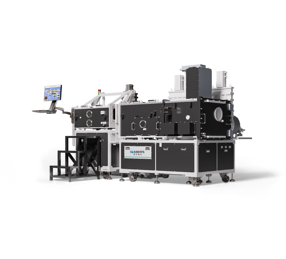
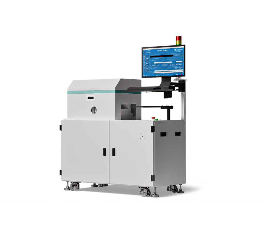
Core Equipment: SAB961X Fully Automatic Super-Atoms Beam TRIM Equipment
- Wafer size: up to 12 inch
- Removal rate: ≥ 400 Å·cm²/s @SiO₂
- Beam current: > 100 μA @Ar
- Cluster ion energy: 60 keV
- SAB961X-Fully automatic
- Super-atoms Beam TRIM Equipment

-
- Core Process 2:Heterogeneous Integration Bonding
Process Capabilities
- Hydrophilic bonding (C2W/W2W) is suitable for integrating LNOI, InP, etc. with silicon photonic wafers.
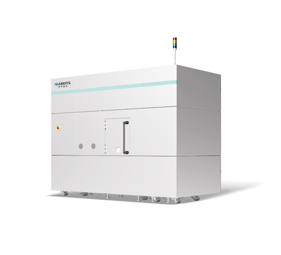
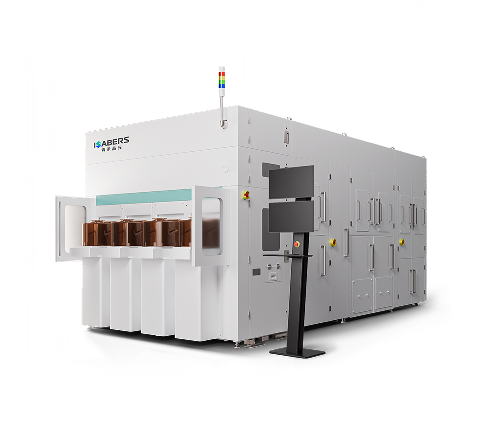
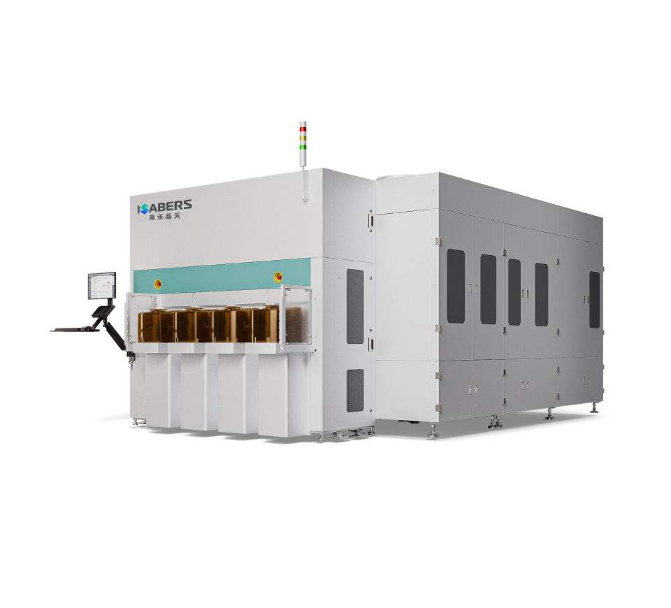
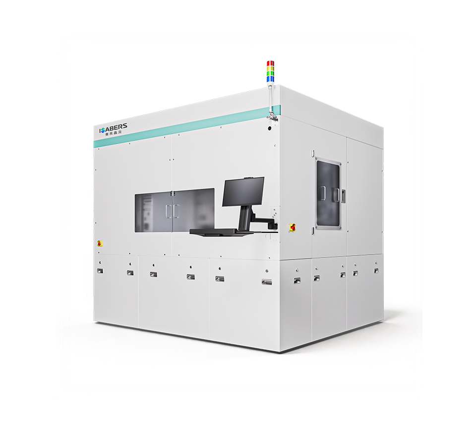
Core Equipment: SAB6210/SAB8210CW Fully Automatic W2W/C2W Hydrophilic Bonding Equipment
- Bonding accuracy: ±50 μm @W2W edge alignment, ±3 μm @C2W chip edge alignment
- C2W bonding equipment is compatible with hybrid bonding, with accuracy < 500 nm
- Chip size: 1×1 mm-32×32 mm
- SAB6210-Fully Automatic
- Hydrophilic Bonding Equipment
-
- Core Process 2:Heterogeneous Integration Bonding
Process Capabilities
- Hydrophilic bonding (C2W/W2W) is suitable for integrating LNOI, InP, etc. with silicon photonic wafers.
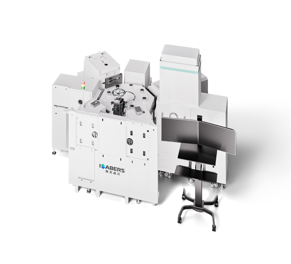
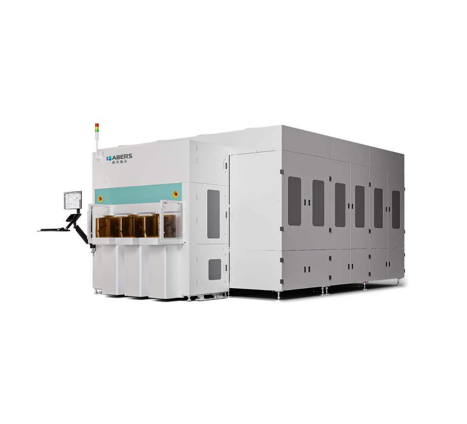
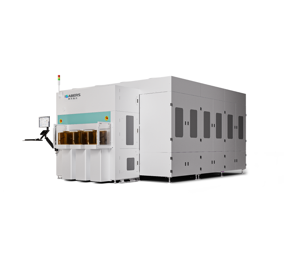
Core Equipment: SAB6210/SAB8210CW Fully Automatic W2W/C2W Hydrophilic Bonding Equipment
- Bonding accuracy: ±50 μm @W2W edge alignment, ±3 μm @C2W chip edge alignment
- C2W bonding equipment is compatible with hybrid bonding, with accuracy < 500 nm
- Chip size: 1×1 mm-32×32 mm
- SAB8210CW-Fully Automatic
- C2W Hybrid Bonding Equipment

- Core Advantages

- Super-atoms Beam TRIM
- Waveguide layer thickness range can be optimized to 1 nm without significantly increasing surface roughness.

- Waveguide Sidewall Polishing
- Eliminates etched sidewall ripples and significantly reduces optical scattering loss.

- High-precision Heterogeneous Bonding
- C2W supports both bare-chip heterogeneous integration and high-precision hybrid bonding of patterned chips.
- Full-process Coverage
- TRIM + polishing + bonding, delivered as a one-stop solution
- Applications
- LNOI high-speed modulators
- Silicon photonics heterogeneous integration (III-V/Si)
- Quantum photonic chips