


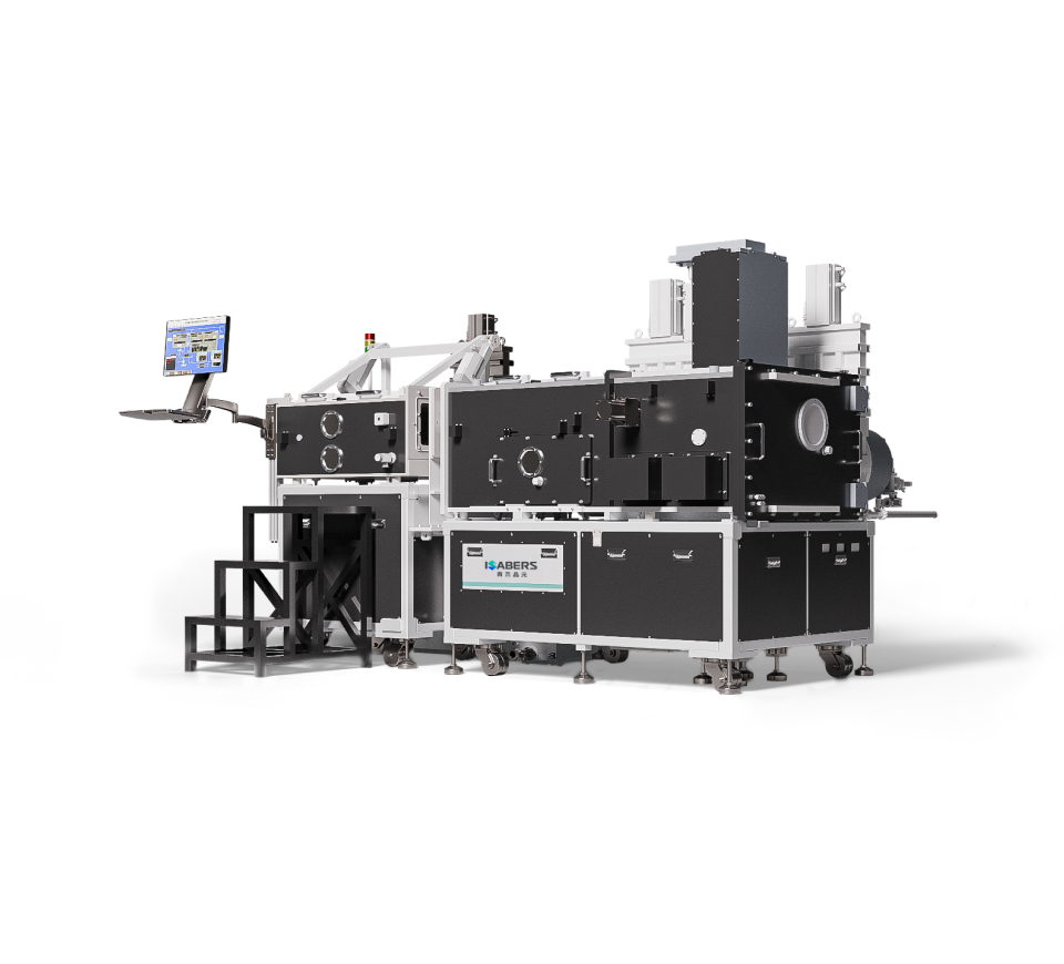
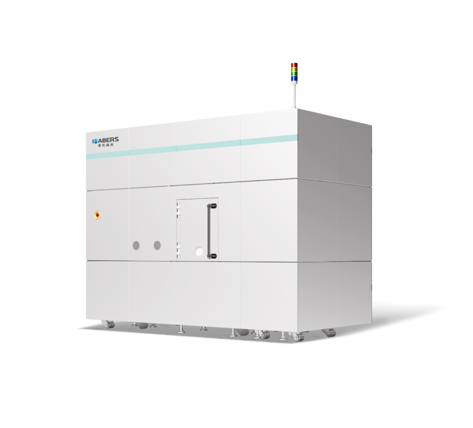
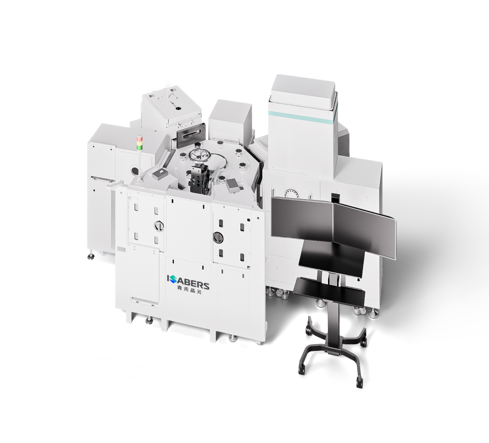
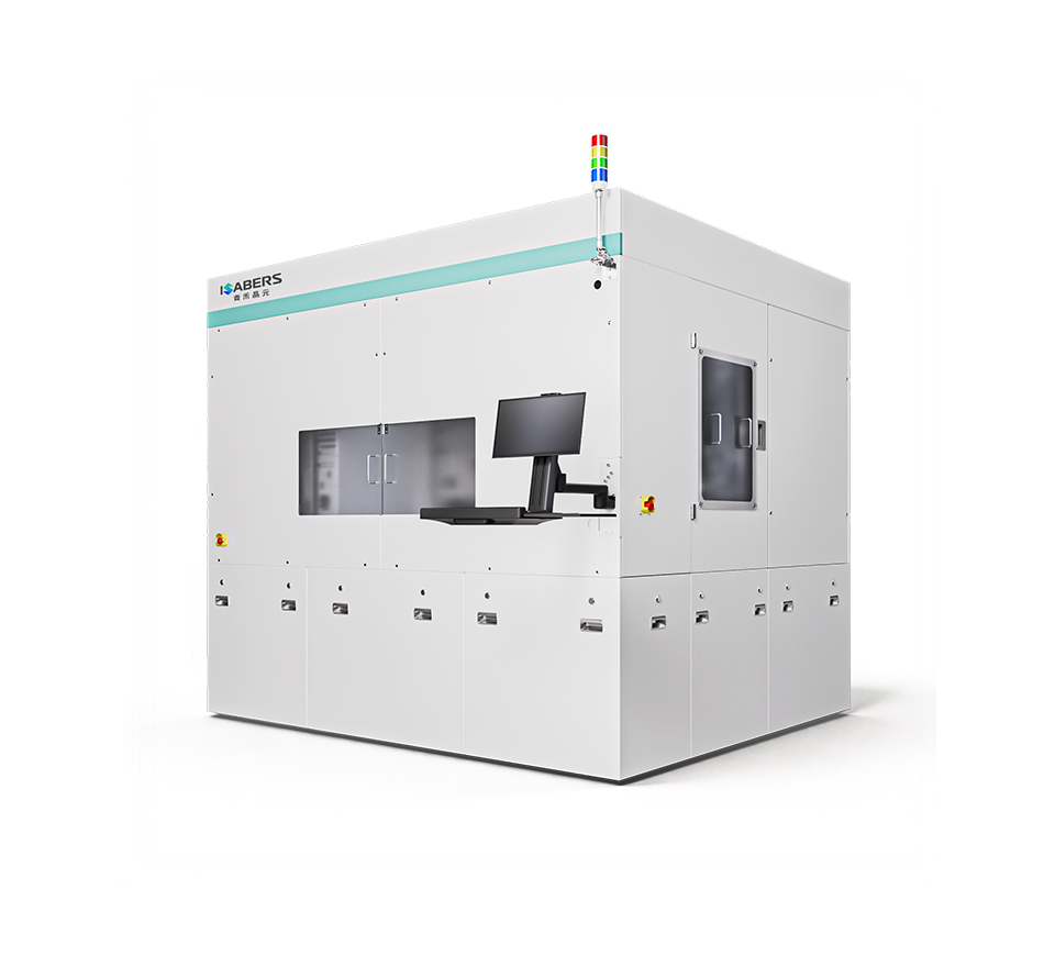
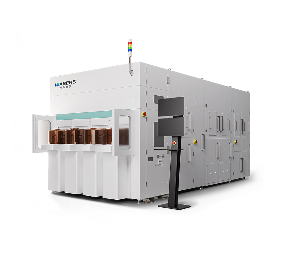
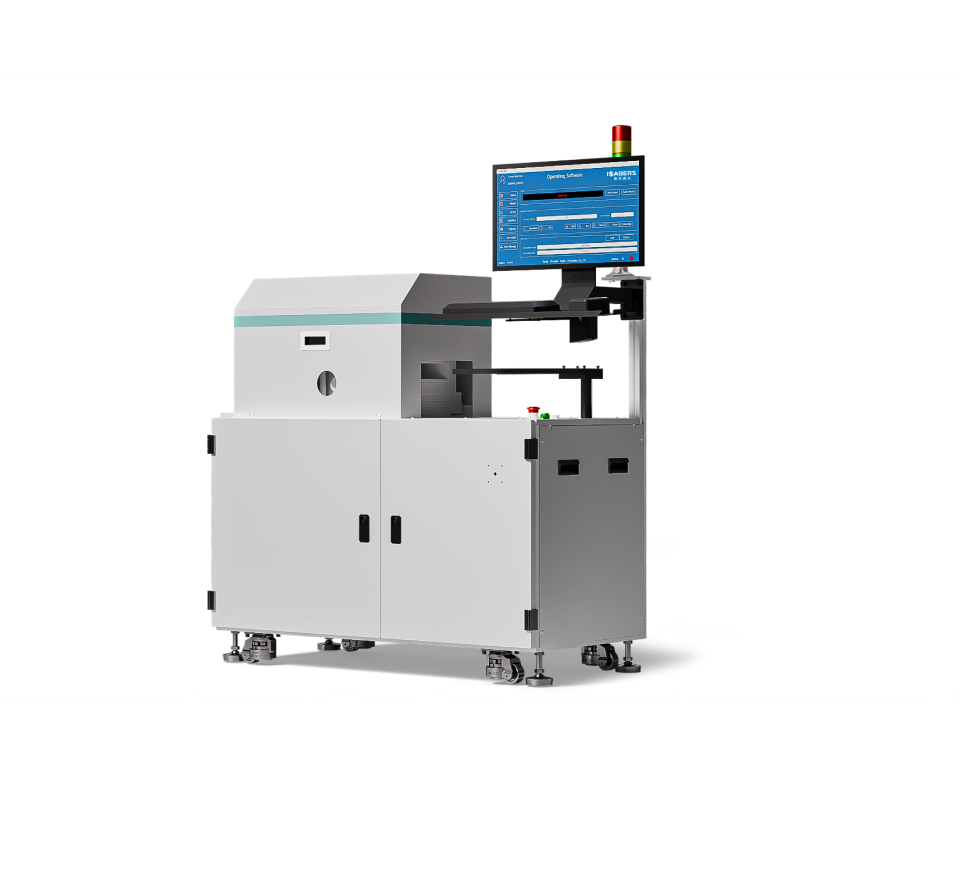
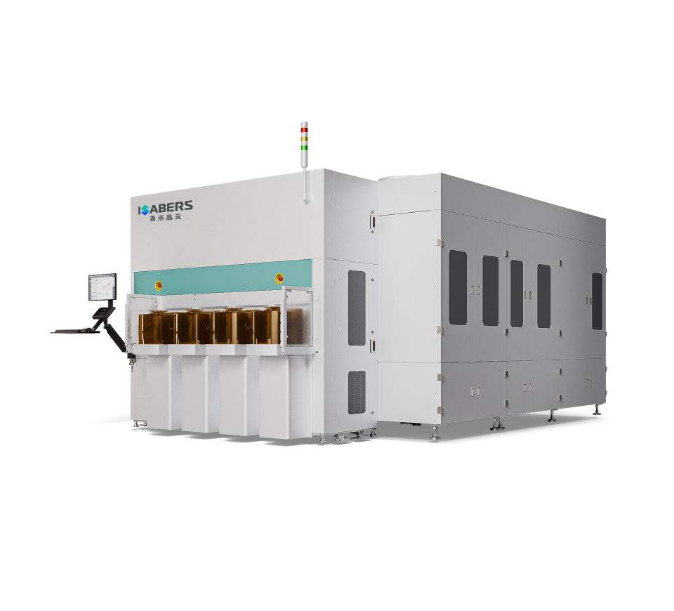
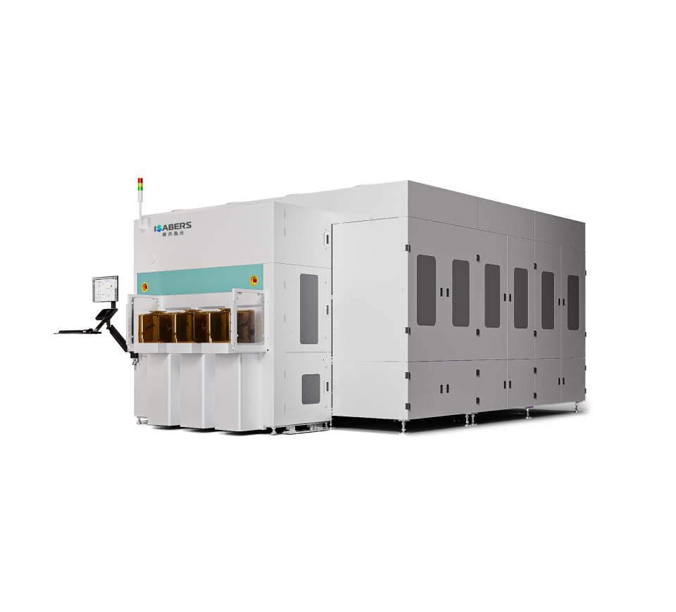
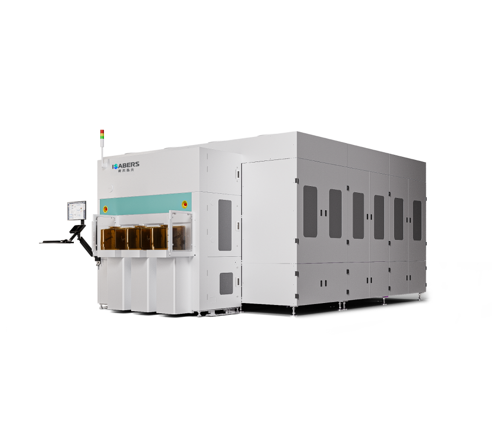







- Based on Self-developed Equipment, Define New Standards for Bonding Materials
Leveraging self-developed bonding equipment, iSABers develops bonding processes for advanced materials including POI acoustic-grade LTOI, TFLN/TFLT, SiCOI, SOI, Emerald-SiC, and mono-SiC on poly-SiC.
These processes have been fully validated on our in-house mass production line, delivering mature process reliability and enabling fast integration into customer lines.
- Advanced Bonding Material Matrix
- Supports a wide range of semiconductor and pan-semiconductor material systems to meet heterogeneous integration requirements.
-

- POI-Acoustic Grade LTOI Substrate
- Consists of a high-resistivity silicon substrate, a buried oxide layer as the intermediate layer, and a thin, uniform mono-LT (Monocrystalline Lithium Tantalate) film on top.
-

- TFLN/TFLT Substrate
- TFLN/TFLT (Thin-Film Lithium Niobate/Tantalate on Insulator) are high-quality monocrystalline thin films fabricated via the H-Cut process.
-

- SiCOI Substrate
- SiCOI (Silicon Carbide-on-Insulator engineered wafer) leverages a proprietary fabrication process to fully exploit the intrinsic properties of High-Purity Semi-Insulating (HPSI) SiC, significantly enhancing the overall performance of semiconductor devices (e.g., high Q-factor).
-

- SOI Substrate
- SOI (Silicon on Insulator) forms a semiconductor thin film on an insulator through wafer bonding and thinning process.
-

- H-CUT SOI Substrate
- H-Cut SOI (Silicon on Insulator) incorporates a silicon dioxide layer between the top silicon layer and the substrate material, forming a semiconductor thin film on the insulator via the H-Cut technology.
-

- Emerald-SiC Engineered Substrate
- Emerald-SiC is a P-grade/D-grade SiC engineered substrate achieved through our innovative advanced wafer bonding and layer transfer technologies.
-

- Mono-SiC on Poly-SiC Engineered Substrate
- Mono-SiC on Poly-SiC Engineered Substrate is achieved by transferring a P-grade mono-SiC film onto a poly-SiC substrate through our innovative advanced wafer bonding and layer transfer technologies, thereby creating a low-resistivity SiC engineered substrate.
-

- HPSI SiC Engineered Substrate
- HPSI SiC engineered substrate is P-grade/D-grade SiC engineered substrate achieved through advanced wafer bonding and layer transfer technologies.
-

- Si on SiC Engineered Substrate
- Si (Silicon) on SiC (Silicon Carbide) engineered substrate, fabricated via bonding and thinning or H-Cut technology.
-

- Ultra-flat Si Wafer
- Through precision thinning and polishing techniques, Si substrates with TTV <0.5 μm are fabricated, enabling high-precision machining processes and advanced process nodes while reducing optical distortion and energy loss.
-

- Diamond on Si Engineered Substrate
- diamond's thermal advantages demonstrate significant value in core fields such as high-end chips, 2.5D/3D advanced packaging, etc.
-

- Other Heterogeneous Materials
- Diamond, InP, GaAs, GaO, GaN and other H-CUT engineered materials.