







- Core Solutions
-
Targeting bonding challenges in MicroLED manufacturing, iSABers offers full-process bonding solutions covering multiple technology routes such as flip-chip bonding, room-temperature bonding, and hybrid bonding, meeting the mass production requirements of various applications including pixel vehicle light, AR displays, and optical communications.
Core Process 1:C2C/C2W Flip-chip Bonding

-
Process Capability
- Eutectic bonding (Au-Sn, Au-In) or metal bonding (Au-Au, Cu-Cu) for flip-chip interconnection between LED chips and CMOS wafers.
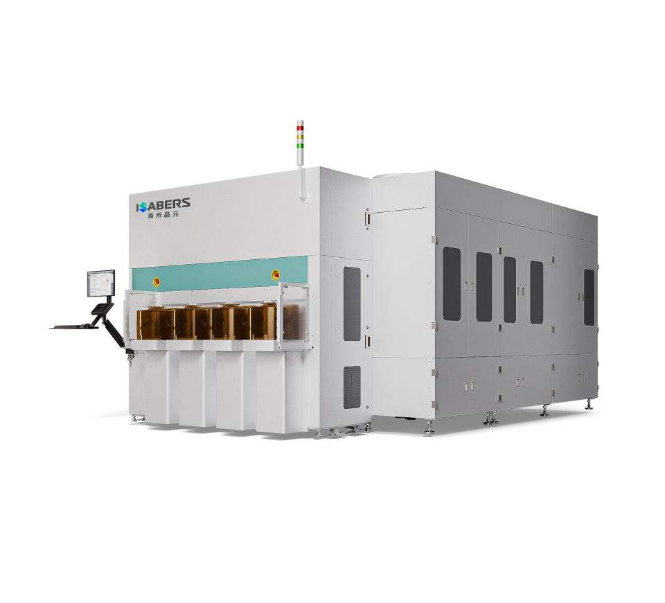
Core Equipment: SAB83 Series C2C & C2W TCB Bonding Equipment
- Supports C2C (R&D/small batch) and C2W (high volume)
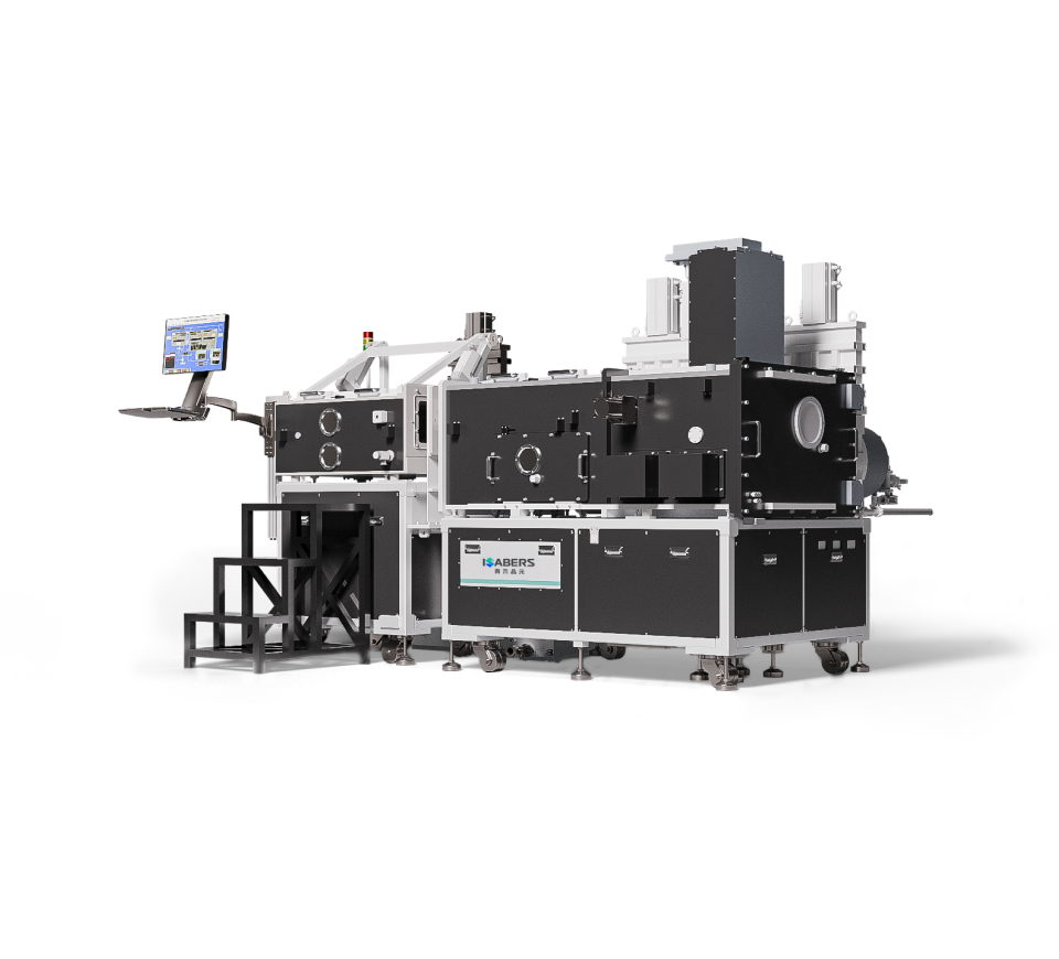
SAB8300 Semi-automatic C2C TCB Bonding Equipment
- Pressure range: 1–3000 N (1–50 N, accuracy ≤ ±0.5 N; 51–3000 N, accuracy ≤ ±2 N)
- Post-bonding accuracy ≤ ±300 nm
- Bond head temperature control: Heating rate ≤ 2.2 s (RT–450°C)
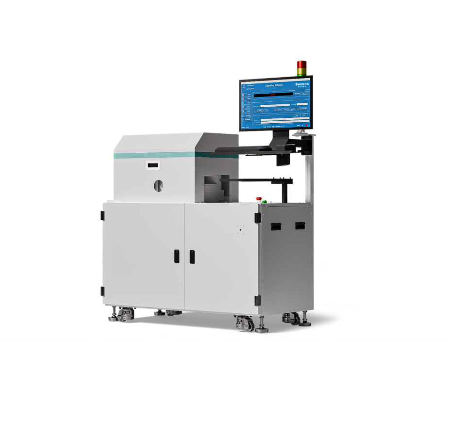
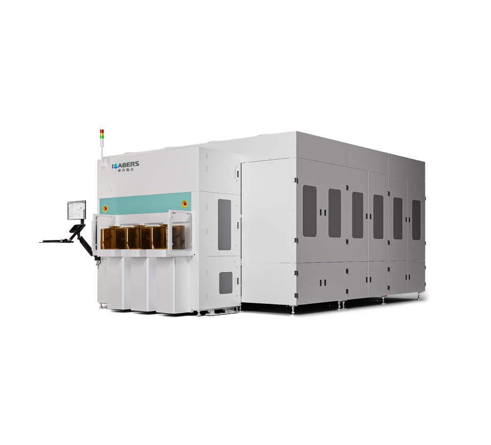
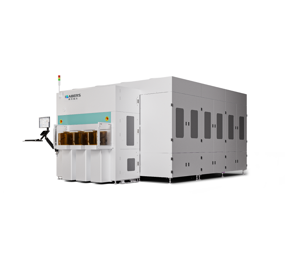
SAB8310 CW Fully Automatic C2W TCB Bonding Equipment
- Pressure range: -30–3000 N (Option 1: -30–500 N, accuracy 0.25 N or 1%; Option 2: 10–3000 N, accuracy ±2 N)
- Post-bonding accuracy ≤ ±500 nm
- Bond head temperature control: Heating rate ≤ 2.2 s (RT–450°C)
- SAB8300-Semi-automatic
- C2C TCB Bonding Equipment

-
Process Capability
- Eutectic bonding (Au-Sn, Au-In) or metal bonding (Au-Au, Cu-Cu) for flip-chip interconnection between LED chips and CMOS wafers.
Core Equipment: SAB83 Series C2C & C2W TCB Bonding Equipment
- Supports C2C (R&D/small batch) and C2W (high volume)
SAB8300 Semi-automatic C2C TCB Bonding Equipment
- Pressure range: 1–3000 N (1–50 N, accuracy ≤ ±0.5 N; 51–3000 N, accuracy ≤ ±2 N)
- Post-bonding accuracy ≤ ±300 nm
- Bond head temperature control: Heating rate ≤ 2.2 s (RT–450°C)
SAB8310 CW Fully Automatic C2W TCB Bonding Equipment
- Pressure range: -30–3000 N (Option 1: -30–500 N, accuracy 0.25 N or 1%; Option 2: 10–3000 N, accuracy ±2 N)
- Post-bonding accuracy ≤ ±500 nm
- Bond head temperature control: Heating rate ≤ 2.2 s (RT–450°C)
- SAB8310CW-Fully Automatic
- C2W TCB Bonding Equipment

Core Process 2:W2W Metal Bonding – Room-temperature Bonding

-
Process Capability
- Room-temperature bonding achieves a bonding layer thickness of only ~10 nm (vs. hundreds of nm for eutectic bonding), reducing etch difficulty and enabling higher pixel density.
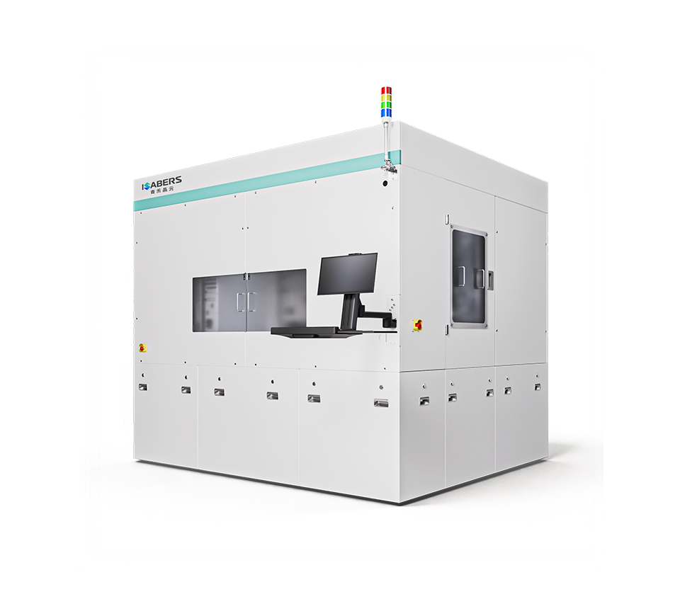
Core Equipment: SAB6110 Fully Automatic UHV RT Bonding Equipment
- Room-temperature direct bonding, no heating needed, eliminating thermal stress
- Full-size compatible bonding
- Precision alignment and pressure control
- Fully automated control and modular design
- High adaptability, enabling flexible control and design of the bonding intermediate layer
- SAB6110-Fully Automatic
- UHV RT Bonding Equipment
Core Process 3:Collective W2W Hybrid Bonding

-
Process Capabilities
- W2W hybrid bonding: vertical stacking enables full-color displays with higher resolution
- C2W hybrid bonding: supports KGD selection and is suitable for scenarios with wafer size mismatch
- Collective W2W hybrid bonding: C2W reconstitution + W2W bonding for higher efficiency
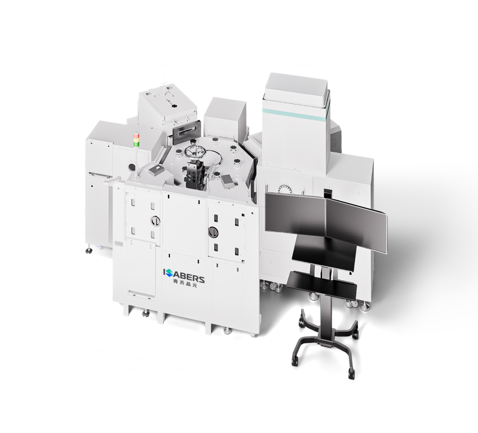
Core Equipment: SAB6210 HB, SAB8210CW/CWW Fully Automatic Hybrid Bonding Equipment
- Supports 8/12 inch wafers
- W2W bonding accuracy ≤ 100 nm / C2W bonding accuracy ≤ 200 nm
- The 8210CWW supports integrated C2W + W2W dual-mode operation
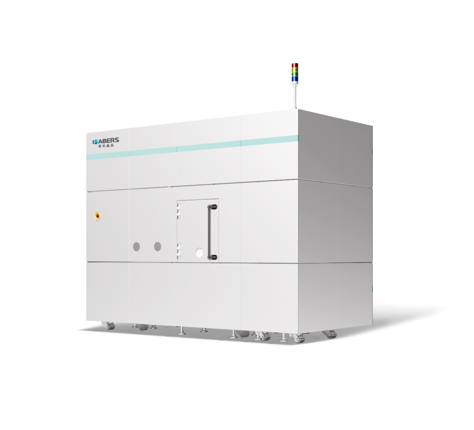
- SAB6210 HB-Fully Automatic
- W2W Hybrid Bonding Equipment
-
Process Capabilities
- W2W hybrid bonding: vertical stacking enables full-color displays with higher resolution
- C2W hybrid bonding: supports KGD selection and is suitable for scenarios with wafer size mismatch
- Collective W2W hybrid bonding: C2W reconstitution + W2W bonding for higher efficiency
Core Equipment: SAB6210 HB, SAB8210CW/CWW Fully Automatic Hybrid Bonding Equipment
- Supports 8/12 inch wafers
- W2W bonding accuracy ≤ 100 nm / C2W bonding accuracy ≤ 200 nm
- The 8210CWW supports integrated C2W + W2W dual-mode operation
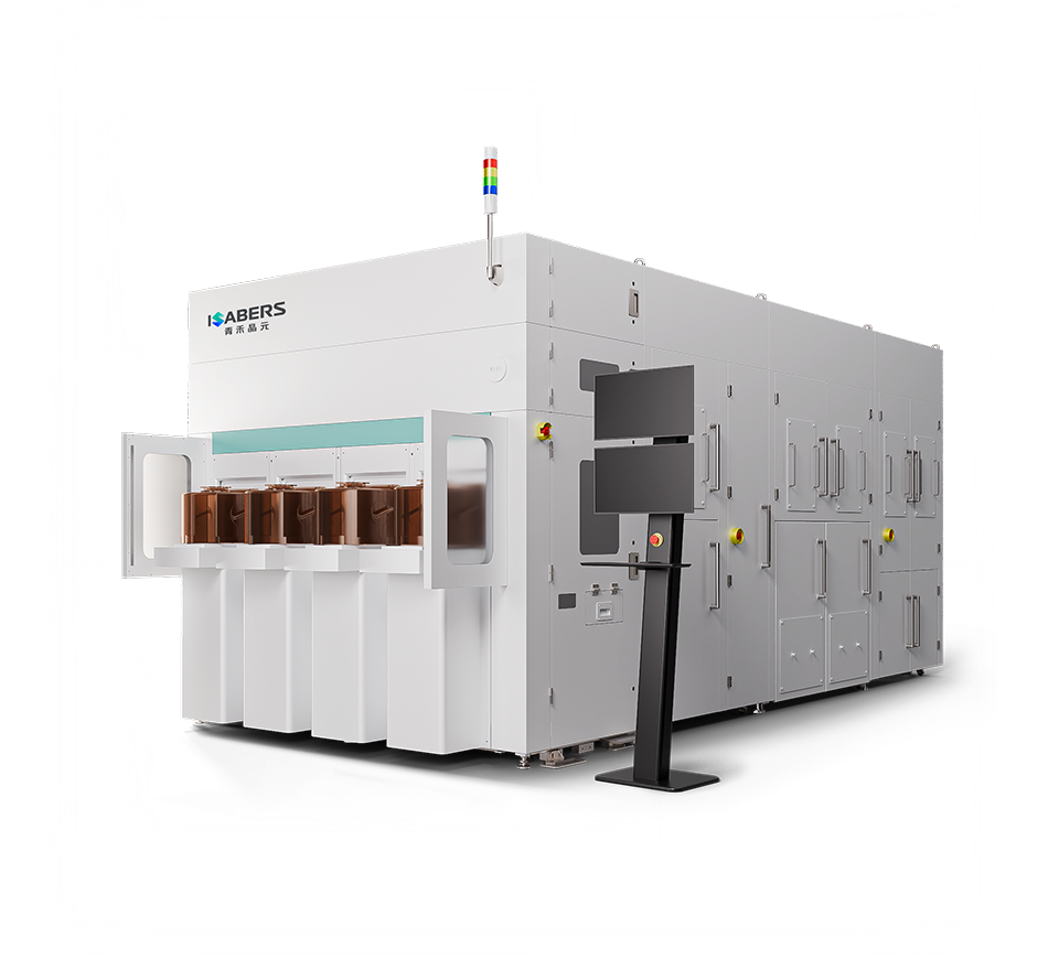
- SAB8210CWW-Fully Automatic
- C2W/W2W Hybrid Bonding Equipment

Core Process 4:Epi Layer Transfer

-
Process Capabilities
- Transfer GaN epi layers from the original substrate to a (100) ultra-flat Si substrate. Ultra-flat Si offers higher mechanical strength and lower TTV (within 0.5 μm), improving downstream process yield.
Core Equipment: SAB6110 Fully Automatic UHV RT Bonding Equipment
- Room-temperature direct bonding, no heating needed, eliminating thermal stress
- Full-size compatible bonding
- Precision alignment and pressure control
- Fully automated control and modular design
- High adaptability, enabling flexible control and design of the bonding intermediate layer
- SAB6110-Fully Automatic
- UHV RT Bonding Equipment
- Core Advantages

- Full-process Coverage
- Flip-chip bonding, room-temperature bonding, and hybrid bonding.

- Advantages of Metal Room-temperature Bonding
- Bonding layer of only ~10 nm, reducing etch difficulty.

- Room-temperature Bonding Enables Epi Layer Transfer
- Reduces bonding stress and improves downstream process yield.
- Wafer Size Matching Solution
- C2W reconstitution + W2W bonding, supporting 4/6/8-inch LED + 8/12-inch CMOS.
- Applications
- Pixel vehicle light (flip-chip bonding)
- AR glasses (room-temperature bonding, hybrid bonding)
- MicroLED full-color displays