


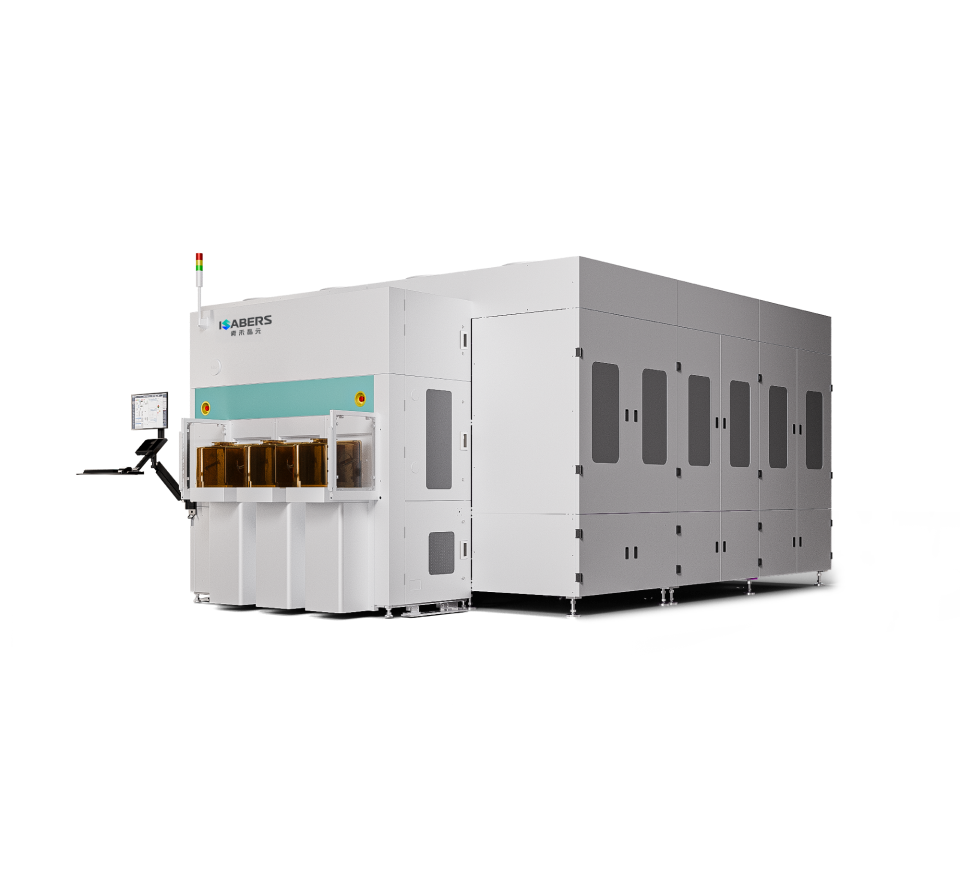







Turnkey Line Design
- Turnkey Solutions · From Equipment to Mass Production Implementation
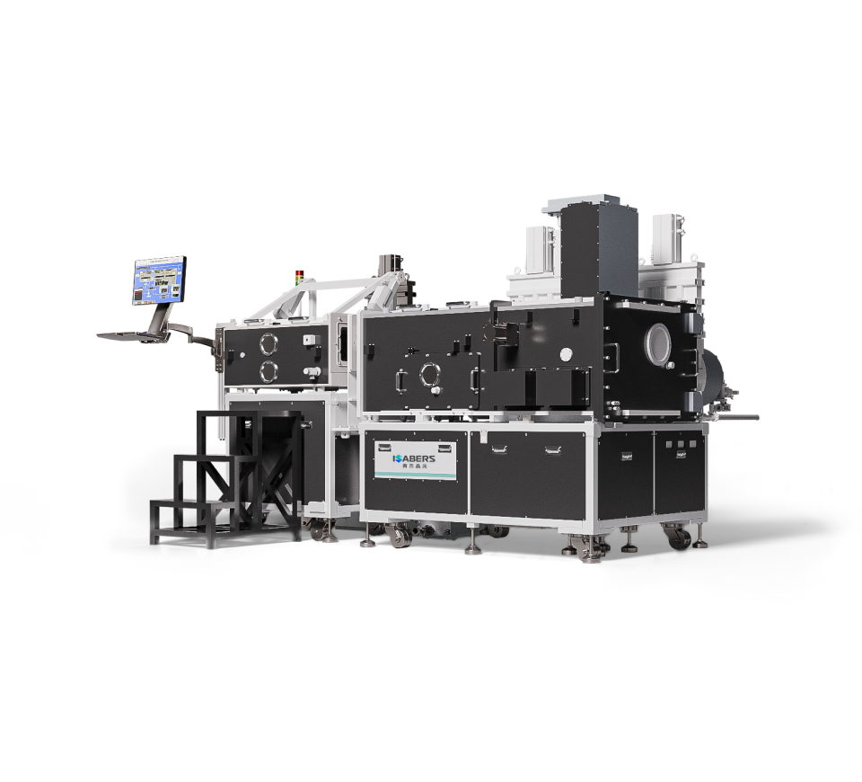
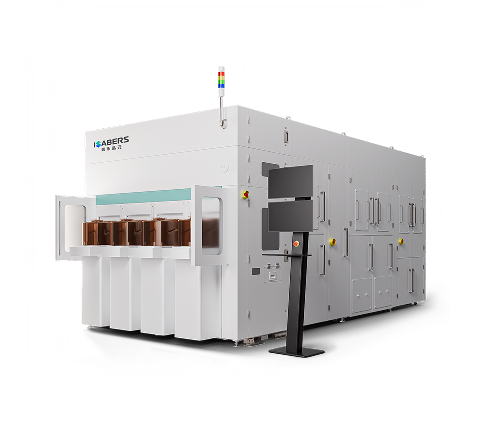
- Self-developed core equipment, custom-designed core process equipment, and coordinated supporting equipment integration — covering ion implantation → bonding → super-atoms beam trim → cleaning → oxidation/poly → splitting/annealing, a complete closed-loop process.
Process Empowerment: H-CUT Process Route / GRD+TRIM Process Route · Mass Production Implementation · Technology Iteration
- Ion Implantation
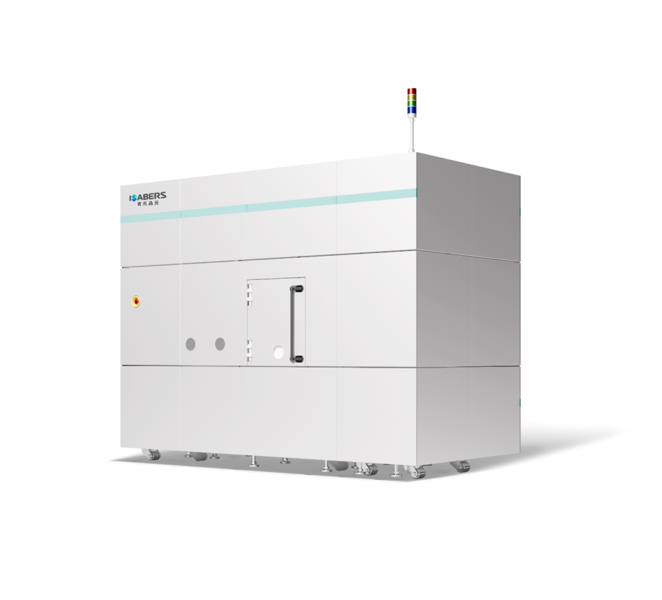
- Designed for 6/8 inch wafer doping, this system uses a metal ion source and a mass analysis magnet to achieve ion implantation such as H⁺ and He. It supports high-throughput implantation of multiple wafers (25 wafers/batch), with dose uniformity of ≤0.3%, and is compatible with various materials with thicknesses of 350-700 μm, ensuring high productivity and implantation stability.
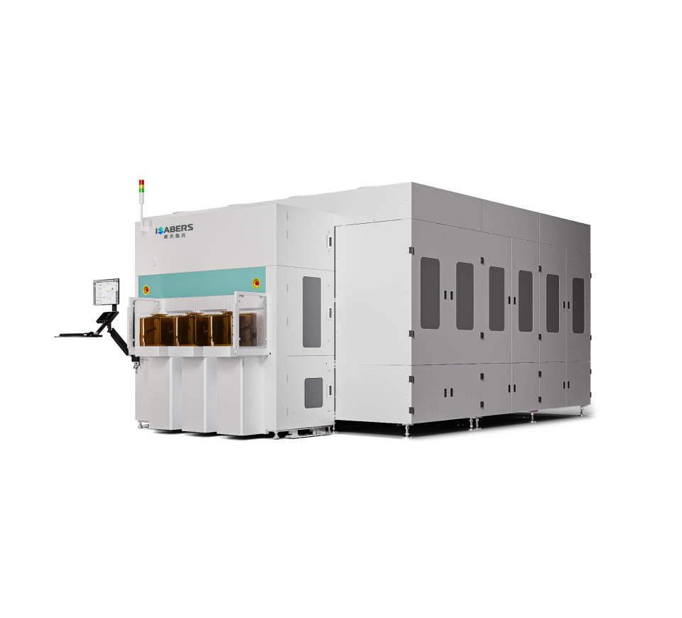
- Bonding Equipment
- UHV RT Bonding Equipment (<5E-6 Pa) removes oxide films via argon atom/ion bombardment and sputter-deposits nanoscale films, enabling atomic-level robust bonding at room temperature. With integrated activation and pressurization, it is compatible with heterogeneous integration of multiple materials such as SiC, POI, and flexible electronics.
Hydrophilic Bonding uses plasma activation to form hydroxyl groups (-OH), followed by room-temperature pre-bonding and annealing to achieve high-strength bonding and Cu-Cu interconnection. It is applied in TFLN / POI / SOI engineered substrates, heterogeneous integration, MEMS capping, and 3D stacking interconnection.
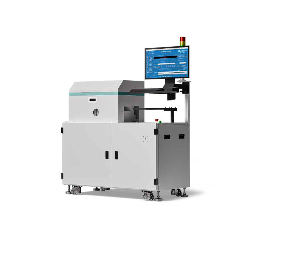
- Associated Test Equipment
- The fully automatic flatness tester employs laser interferometry for non-contact measurement of wafer TTV/TIR and warpage, ensuring bonding surface alignment accuracy. The ultrasonic microscope uses high-frequency ultrasound to non-destructively detect internal defects such as delamination and voids at the bonding interface. Based on reflective spectroscopy, the fully automated film thickness measurement system precisely monitors film thickness and uniformity. Together, they ensure comprehensive bonding quality control.
- Super-atoms Beam Trim
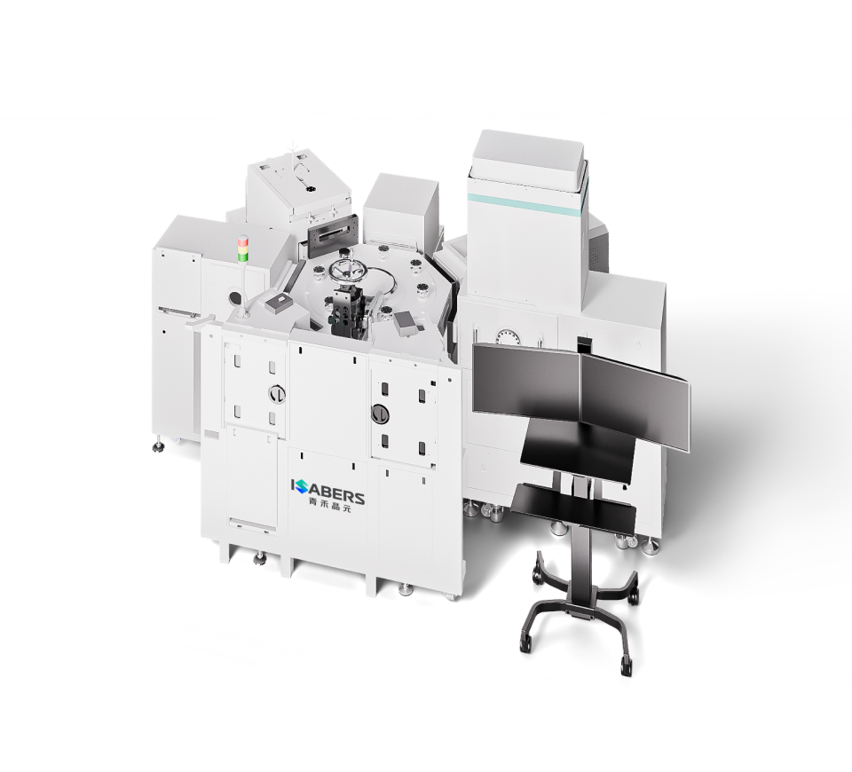
- Based on gas-based super-atoms beam technology, the process enables low-damage, atomic-level surface planarization etching. With lateral sputtering and a high removal rate, it precisely corrects film thickness non-uniformity on wafer surfaces. Ideal for frequency correction and surface modification of SAW/BAW filters, it improves device performance and consistency.
- Oxidation Furnace
- Designed for dry/wet oxidation processes to grow high-quality SiO₂ layers, this system features a vertical five-zone temperature control system with cascade PID control and is compatible with both non-transparent and transparent wafers. It achieves a single-batch film thickness of up to 1.2 μm, offering excellent thick-oxide growth capability. Suitable for gate oxide layers, isolation layers, sacrificial layers, etc., it is a key tool for device insulation and doping barriers.
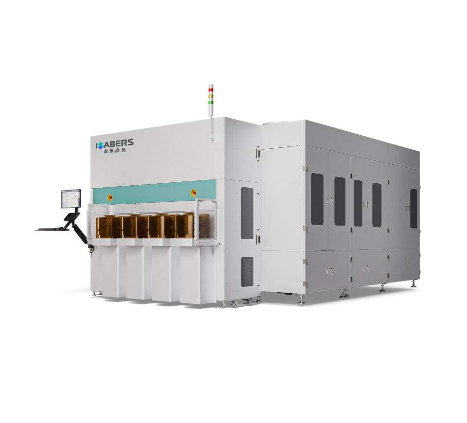
- Cleaning Equipment
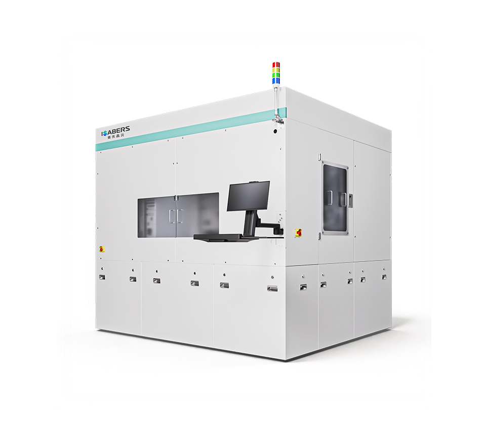
- A high-precision wet cleaning system designed for 2-12 inch Si wafers and compound semiconductor substrates, processing one wafer at a time in an independent sealed chamber. It features PVA Brush (high moisture absorption, high elasticity, wear resistance, and anti-static) and Mega-sonic nozzles (micro-jet effect for efficient removal of non-nanoparticles with low damage), combined with custom swing-arm scanning to achieve highly uniform cleaning and drying. It is a key tool for ensuring front-end yield in processes such as bonding and etching.


Process Route & Mass Production Implementation
Equipment + Materials + Process Integration for Rapid Mass Production
- H-CUT Process RouteEnables the bonding of 200–600 nm (LN) and 200–1000 nm (LT) monocrystalline thin films with silicon-based substrates, with LN/LT & BOX film thickness controlled within ±1%; enables the fabrication of 0.1–1.5 μm SOI with device-layer thickness uniformity of <20 nm; enables the transfer of high-quality mono-SiC thin layers onto low-cost SiC substrates, with a transferred high-quality layer thickness of >0.5 μm.
- GRD+TRIM Process RouteHigh-precision surface treatment ensures perfect compatibility of the bonding interface and enables the fabrication of thick-film bonded substrates.
Process Tuning, Mass Production Implementation, and Technology Iteration, End-to-End Support from Lab to Fab.
Full Application Coverage
- New Material Mass Production Line
- Expansion and Upgrade of Existing Production Lines
- University / Research Institute Laboratories
- New Material Pilot Line
- Why Choose iSABers' Turnkey Solutions?
- We deliver not just a single piece of equipment, but a mass production line that is tuned to your material, configured to your process, and validated for your capacity.
Turnkey Delivery. We Take Full Responsibility for Achieving Production.
-


- Leading Materials
- LTOI / LNOI / POI / SiC / SOI engineered substrates deliver performance on par with global leaders and have been validated by tier-1 customers.
-


- Independent & Secure Equipment
- Core equipment is self-developed and self-manufactured, while processing equipment is custom-selected to ensure supply chain security and delivery schedules.
-


- Integrated Process Coupling
- Upstream and downstream equipment are deeply coupled, eliminating the long matching cycles, selection errors, and high trial-and-error costs of building a line yourself.
-


- Mature Processes
- Full-process validation with film thickness control within ±1% ensures stable mass production output.
-


- Efficient Line Deployment
- Short equipment lead times and fast process integration significantly shorten line construction, helping customers accelerate time-to-market and revenue.
-


- Patent Portfolio + Professional Team
- A proprietary IP portfolio effectively mitigates technology restrictions; three-stage validation and simulation ensure closed-loop implementation.
 Tianjin Advanced Bonding Materials R&D & Production Line