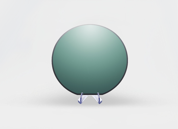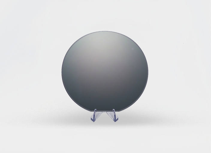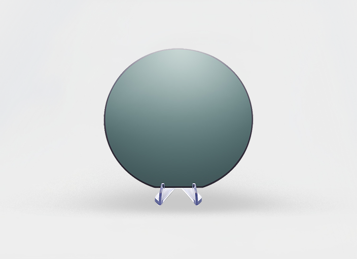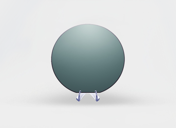



TFLN/TFLT Substrate
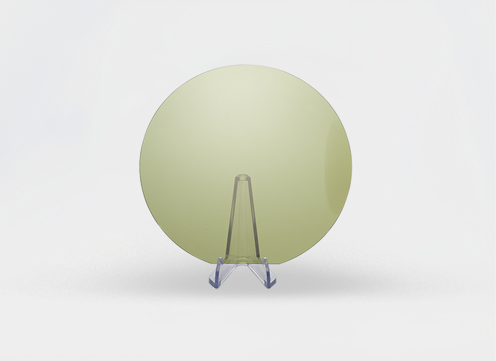
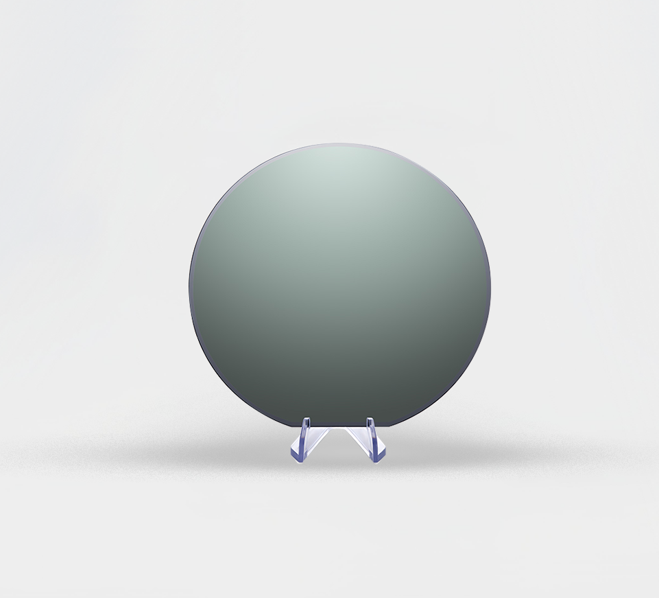
TFLN/TFLT (Thin-Film Lithium Niobate/Tantalate on Insulator) are high-quality monocrystalline thin films fabricated via the H-Cut process. Leveraging its exceptional electro-optic properties (r₃₃ ≈ 30-80 pm/V), TFLN has become the material of choice for high-speed optical modulators (100 GHz+) and quantum photonic devices. Its strong second-order nonlinearity (χ⁽²⁾) enables efficient wavelength conversion and entangled photon pair generation. It has been validated by leading domestic optical module companies and has secured overseas tier-one customers. TFLT offers superior broadband transparency, making it ideal for mid-infrared sensing applications. With a higher optical damage threshold (>500 MW/cm²) and excellent thermal stability (dn/dT ≈ 1.5×10⁻⁵/K), TFLT excels in high-power optical systems. Both materials are compatible with CMOS processes. TFLN focuses on high-speed communications and quantum optics, while TFLT shines in infrared optoelectronics and acousto-optic hybrid systems. Together, they drive advances in next-generation integrated photonic devices.
TFLN (TFLT) Substrate (6 inch)
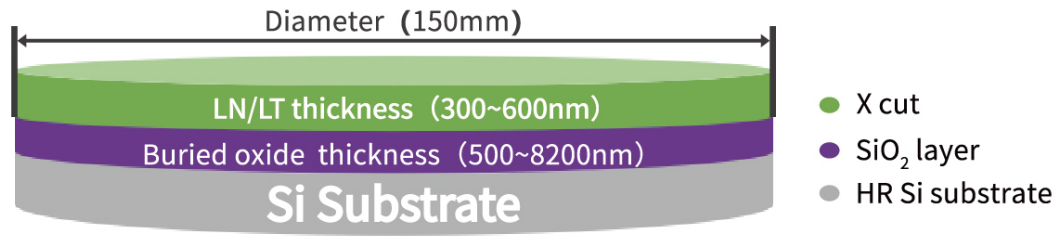
  • Items
  • Specification
  • Diameter
  • 150±0.2 mm
  • LN/LT Crystal Orientation
  • X°±0.3°
  • LN/LT Layer Thickness
  • (300~600 nm) ±20 nm
  • Front Side Surface Finish
  • <0.5 nm
  • Buried Oxide Layer Thickness
  • (500~8200 nm) ±20 nm
  • Si Orientation
  • <100>
  • TTV
  • ≤5 μm
  • BOW
  • -40~40 μm
  • Warp
  • ≤50 μm
  • Total Thickness
  • 675±25 μm


TFLN (TFLT) Substrate (8 inch)
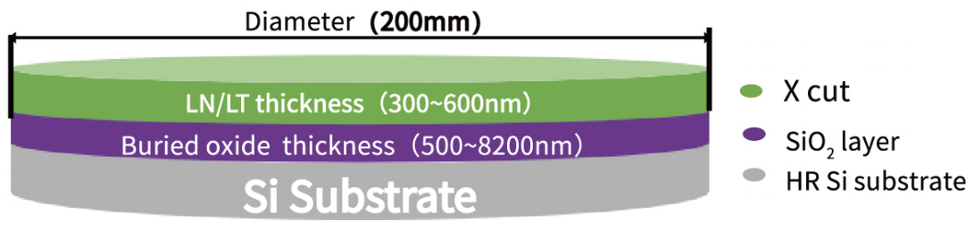
  • Items
  • Specification
  • Diameter
  • 200±0.2 mm
  • LN/LT Crystal Orientation
  • X°±0.3°
  • LN/LT Layer Thickness
  • (300~600 nm)±20 nm
  • Front Side Surface Finish
  • <0.5 nm
  • Buried Oxide Layer Thickness
  • (500~8200nm)±20nm
  • Si Orientation
  • <100>
  • TTV
  • ≤5 μm
  • BOW
  • -50~50 μm
  • Warp
  • ≤50 μm
  • Total Thickness
  • 725±25 μm
More cases
Service Email:
sales@isaber-s.com

Address: No. 38, Binhai Innovation and Entrepreneurship Park, No. 4668 Xinbei Road, Binhai New Area, Tianjin

About Us
Company Profile
Development History
Partners
Bonding Equipment
Wafer Bonding Equipment
Chip Bonding Equipment
Surface Treatment Equipment
News
Group News
Events & Exhibitions
Contact Us
Product Inquiries
Investor Inquiries
Join Us
Follow us
Copyright  © 2024 iSABers Group Co., Ltd. |  津ICP备2025028526号 |  津ICP备2022006256号-1