

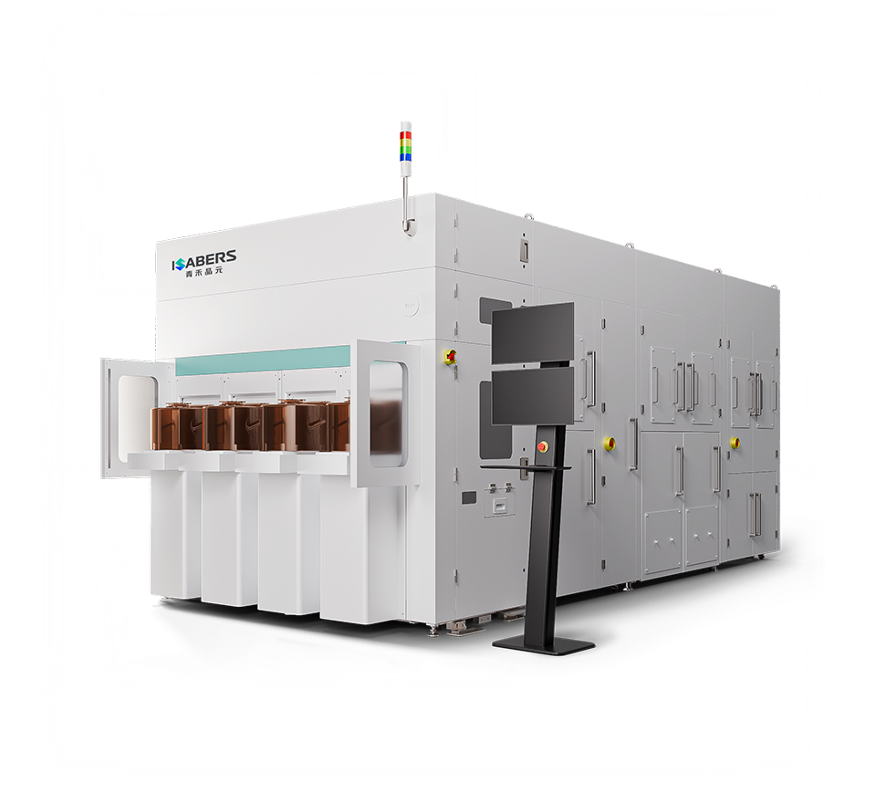
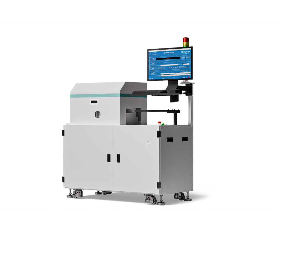
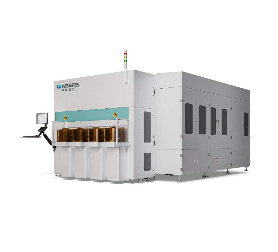
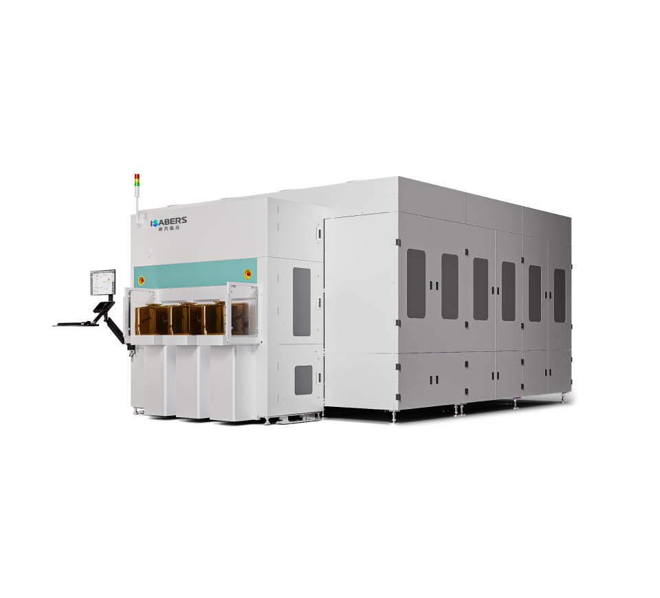
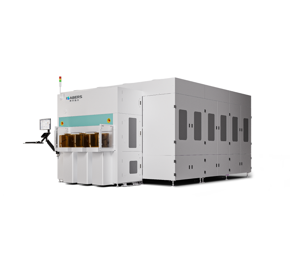



Mono-SiC on Poly-SiC Engineered Substrate
Mono-SiC on Poly-SiC Engineered Substrate is achieved by transferring a P-grade mono-SiC film onto a poly-SiC substrate through our innovative advanced wafer bonding and layer transfer technologies, thereby creating a low-resistivity SiC engineered substrate. This SiC engineered substrate technology can significantly reduce the substrate resistivity while lowering the cost per wafer, ultimately enhancing device performance. It has been validated by leading domestic customers.
Mono-SiC on Poly-SiC Engineered Substrate (6 inch)

  • Items
  • Specification
  • Diameter
  • 150±0.2 mm
  • Pol type
  • 4H
  • Dopant
  • N-type/Nitrogen
  • Face Orientation
  • 4.0° off-axis towards <11-20>±0.5°
  • Transfer Layer Thickness
  • ≥0.5 μm
  • Void (Size: ≥5 mm)

    Void (Size: 1~5 mm)

    Void (Size: 0.5~1 mm)

  • 0 ea/wafer

    ≤3 ea/wafer

    ≤5 ea/wafer

  • Handle Polytype
  • 3C
  • Resistivity
  • ≤0.005 ohm·cm
  • Front (Si-face) Roughness
  • Ra≤0.2 nm (5 μm*5 μm)
  • Edge Chip, Scratch, Crack (visual inspection)
  • None
  • TTV
  • ≤5 μm
  • Warp
  • ≤50 μm
  • Thickness
  • 350±25 μm
Mono-SiC on Poly-SiC Engineered Substrate (8 inch)

  • Items
  • Specification
  • Diameter
  • 200±0.2 mm
  • Polytype
  • 4H
  • Dopant
  • N-type/Nitrogen
  • Face Orientation
  • 4.0° off-axis towards <11-20> ±0.5°
  • Transfer Layer Thickness
  • ≥0.5 μm
  • Void (Size: ≥5 mm)

    Void (Size: 1~5 mm)

    Void (Size: 0.5~1 mm)

  • 0 ea/wafer

    ≤6 ea/wafer

    ≤10 ea/wafer

  • Handle Polytype
  • 3C
  • Resistivity
  • ≤0.005 ohm·cm
  • Front (Si-face) Roughness
  • Ra ≤ 0.2 nm (5 μm * 5 μm)
  • Edge Chip, Scratch, Crack (visual inspection)
  • None
  • TTV
  • ≤7 μm
  • Warp
  • ≤50 μm
  • Thickness
  • 500±25 μm
More cases
Service Email:
sales@isaber-s.com

Address: No. 38, Binhai Innovation and Entrepreneurship Park, No. 4668 Xinbei Road, Binhai New Area, Tianjin

About Us
Company Profile
Development History
Partners
Bonding Equipment
Wafer Bonding Equipment
Chip Bonding Equipment
Surface Treatment Equipment
News
Group News
Events & Exhibitions
Contact Us
Product Inquiries
Investor Inquiries
Join Us
Follow us
Copyright  © 2024 iSABers Group Co., Ltd. |  津ICP备2025028526号 |  津ICP备2022006256号-1