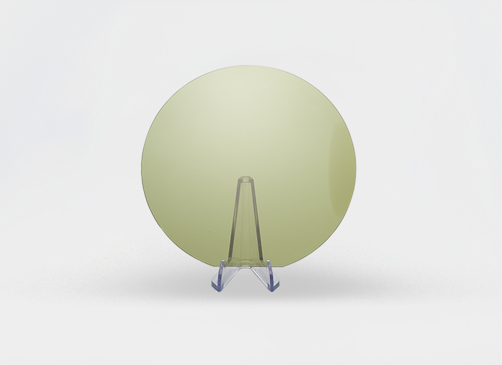









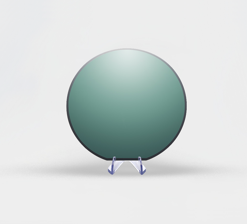
POI-Acoustic Grade LTOI Substrate (H-Cut)
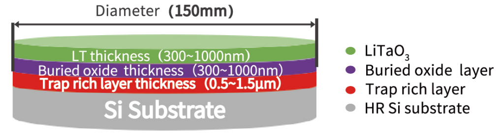
- Items
- Specification
- Diameter
- 150±0.2 mm
- LT Crystal Orientation
- Y36°/Y42°/Y50°±0.3°
- LT Layer Thickness Mean
- (300~1000)±20 nm
- Layer Thickness Range
- <40 nm
- Front Side Surface Finish
- <0.5 nm
- Buried Oxide Layer Thickness Mean
- (300~1000)±20 nm
- Buried Oxide Layer Thickness Range
- <40 nm
- Trap-Rich Layer Average Thickness
- {0.5-1.5 μm}±0.1 μm
- Si Orientation
- <100>, <110> ,<111>, etc.
- TTV
- ≤5 μm
- BOW
- -50~50 nm
- Warp
- <50 μm
- Total Thickness
- 675±25 μm
POI-Acoustic Grade LTOI Substrate (Thinning)
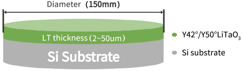
- Items
- Specification
- Diameter
- 150±0.2 mm
- LT Crystal Orientation
- Y36°/Y42°/Y50°±0.3°
- LT Layer Thickness Mean
- (2~50)±0.5 μm
- Layer Thickness Range
- <2 μm
- Front Side Surface Finish
- <0.5 nm
- Si Orientation
- <100>, <110>, <111>, etc
- TTV
- ≤5 μm
- BOW
- -50~50 nm
- Warp
- <50 μm
- Total Thickness
- 675±25 μm
POI-Acoustic Grade LTOI Substrate (Thinning)

- Items
- Specification
- Diameter
- 150±0.2 mm
- LT Crystal Orientation
- Y36°/Y42°/Y50°±0.3°
- LT Layer Thickness Mean
- (300~10000)±50 nm
- Layer Thickness Range
- <100 nm
- Front Side Surface Finish
- <0.5 nm
- Buried Oxide Layer Thickness Mean
- (300~1000)±20 nm
- Buried Oxide Layer Thickness Range
- <40 nm
- Trap-Rich Layer Average Thickness
- {0.5-1.5 μm}±0.1 μm
- Si Orientation
- <100>, <110> ,<111>, etc.
- TTV
- ≤5 μm
- BOW
- -50~50 nm
- Warp
- <50 μm
- Total Thickness
- 675±25 μm