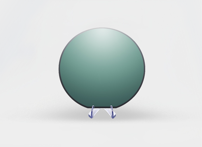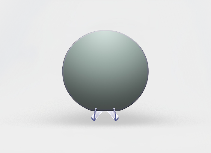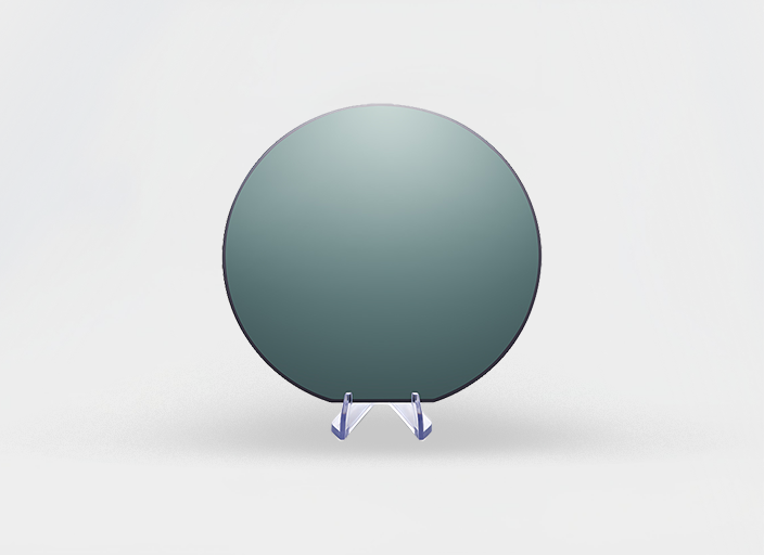




SiCOI Substrate
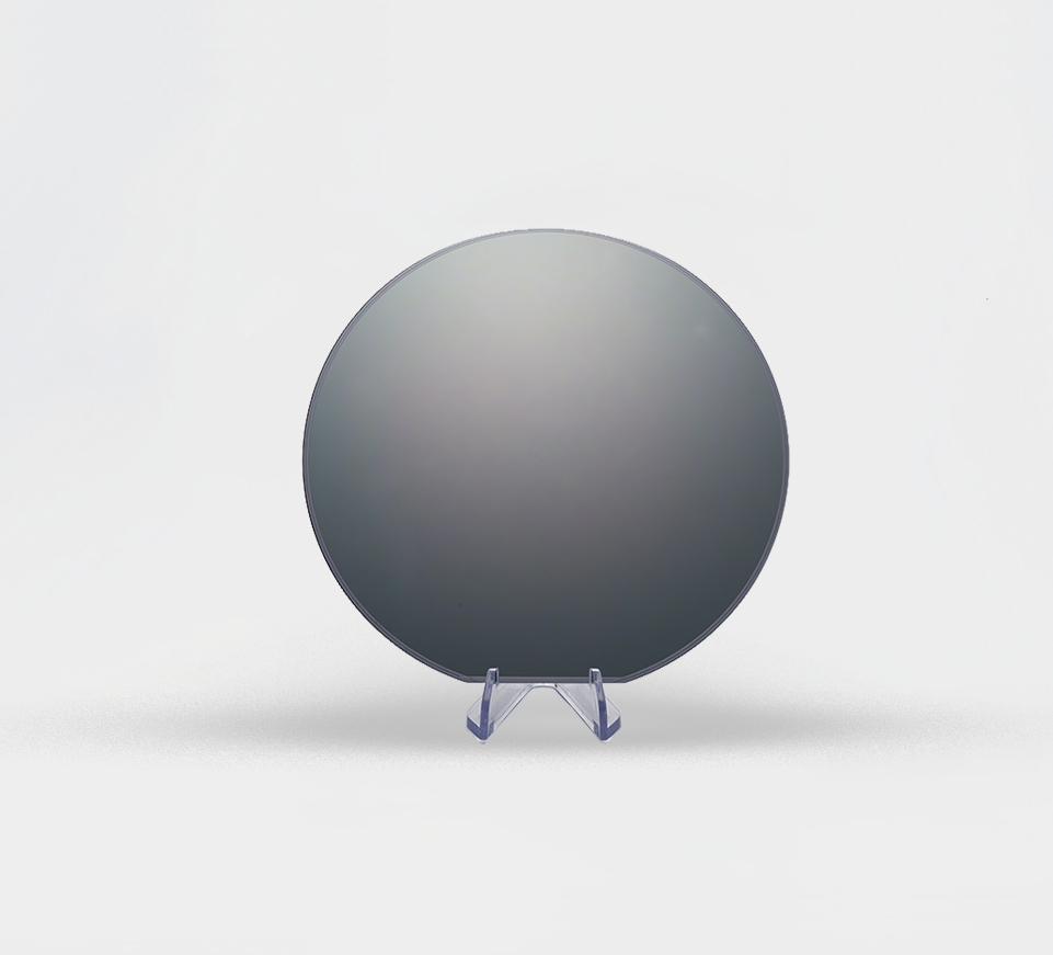
SiCOI (Silicon Carbide-on-Insulator engineered wafer) leverages a proprietary fabrication process to fully exploit the intrinsic properties of High-Purity Semi-Insulating (HPSI) SiC, significantly enhancing the overall performance of semiconductor devices (e.g., high Q-factor). Its outstanding optical properties find critical applications in second harmonic generation, electro-optic modulators, optical frequency combs, PICs, etc.
SiCOI Substrate

  • Items
  • Specification
  • Diameter
  • 150±0.2 mm
  • SiC Polytype
  • 4H
  • SiC Resistivity
  • ≥1E8 ohm·cm
  • SiC Mean Thickness (21 Pts)
  • ≥0.5 μm
  • SiC Thickness Range
  • ≤2000 A
  • Front (C-face) roughness
  • Ra≤0.2 nm (5 μm*5 μm)
  • Oxide thickness
  • (0~3000) ±5% nm
  • SI Orientation
  • <100>, <110>, <111>, etc.
  • Si Type
  • P/N
  • Edge Chip, Scratch, Crack (visual inspection)
  • None
  • TTV
  • ≤5 μm
  • Thickness
  • 500-675 μm
More cases
Service Email:
sales@isaber-s.com

Address: No. 38, Binhai Innovation and Entrepreneurship Park, No. 4668 Xinbei Road, Binhai New Area, Tianjin

About Us
Company Profile
Development History
Partners
Bonding Equipment
Wafer Bonding Equipment
Chip Bonding Equipment
Surface Treatment Equipment
News
Group News
Events & Exhibitions
Contact Us
Product Inquiries
Investor Inquiries
Join Us
Follow us
Copyright  © 2024 iSABers Group Co., Ltd. |  津ICP备2025028526号 |  津ICP备2022006256号-1