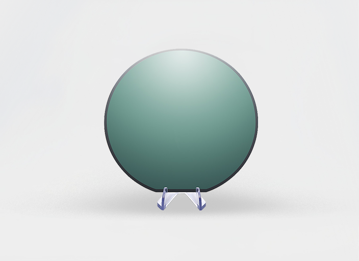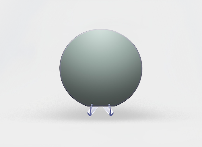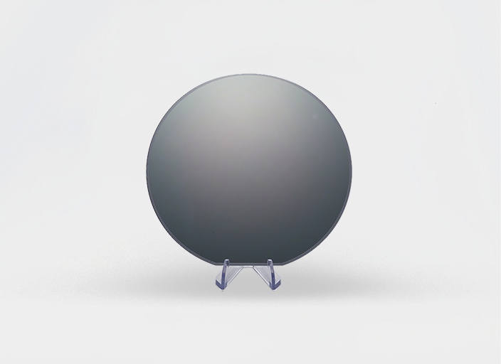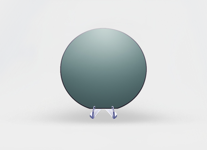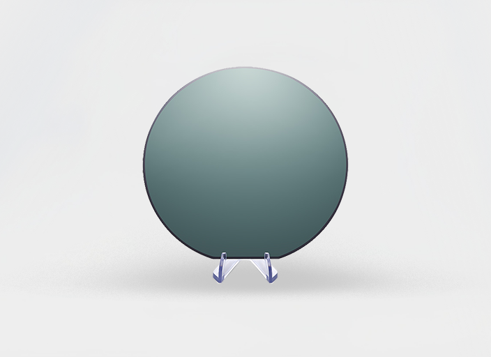



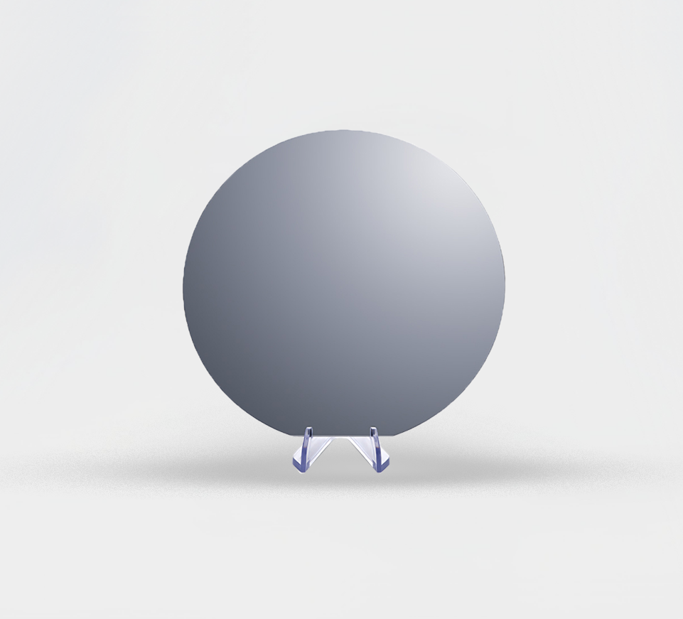
Ultra-flat Si Wafer
Through precision thinning and polishing techniques, Si substrates with TTV <0.5 μm are fabricated, enabling high-precision machining processes and advanced process nodes while reducing optical distortion and energy loss. Thanks to their exceptional thickness uniformity, these substrates play an indispensable role in semiconductor, photovoltaic, optical, and MEMS applications.
Ultra-flat Si Wafer (6, 8 inch)
  • Items
  • Specification
  • Diameter
  • 150±0.2 mm
  • Si Orientation
  • <100>, <110>, <111>, etc.
  • Si Type
  • P/N
  • TTV
  • ≤0.5 μm
  • Front roughness
  • Ra≤0.2 nm (5 μm * 5 μm)
  • Items
  • Specification
  • Diameter
  • 200±0.2 mm
  • Si Orientation
  • <100>, <110>, <111>, etc.
  • Si Type
  • P/N
  • TTV
  • ≤0.5 μm
  • Front roughness
  • Ra≤0.2 nm (5 μm * 5 μm)
More cases
Service Email:
sales@isaber-s.com

Address: No. 38, Binhai Innovation and Entrepreneurship Park, No. 4668 Xinbei Road, Binhai New Area, Tianjin

About Us
Company Profile
Development History
Partners
Bonding Equipment
Wafer Bonding Equipment
Chip Bonding Equipment
Surface Treatment Equipment
News
Group News
Events & Exhibitions
Contact Us
Product Inquiries
Investor Inquiries
Join Us
Follow us
Copyright  © 2024 iSABers Group Co., Ltd. |  津ICP备2025028526号 |  津ICP备2022006256号-1