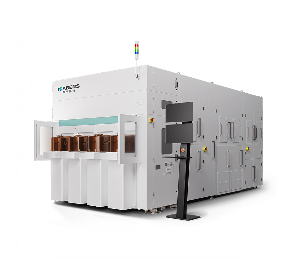
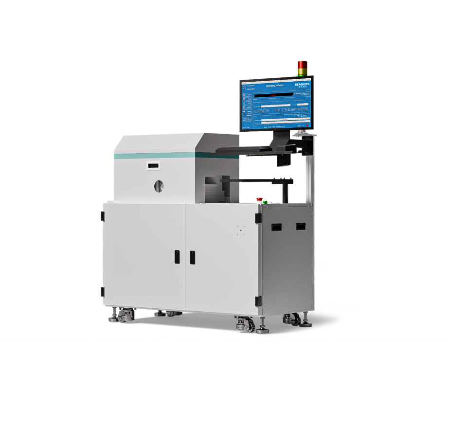
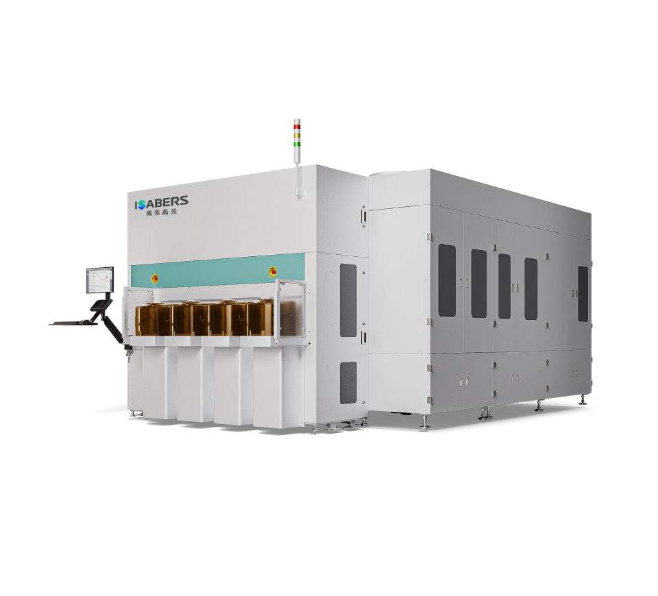
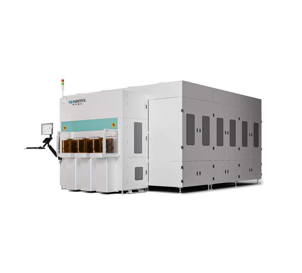
- Diamond on Si Engineered Substrate
Diamond and Si engineered substrate, fabricated via H-Cut technology, by optimizing the implantation and annealing lift-off process conditions to mitigate the thermal mismatch effect between the two materials, has successfully achieved Diamond on Si. As an ultra-high thermal conductivity insulating layer, diamond's thermal advantages demonstrate significant value in core fields such as high-end chips, 2.5D/3D advanced packaging, etc.
Diamond on Si Engineered Substrate
-
Diamond Orientation
-
<001>
-
Diamond Thickness
-
≥0.4 μm
-
Front roughness Ra
-
1~10nm(5 μm*5 μm)